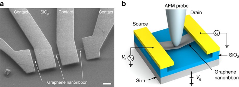
Figure 1. Device and experimental set-up.
(a) Scanning electron microscope (SEM) image of the device. A 60-nm-wide graphene nanoribbon is suspended above a substrate and contacted by electrodes. Scale bar, 500-nm long. (b) Schematic drawing of the experimental set-up and geometry. The suspended graphene ribbon is deformed in the centre using an AFM probe attached to a piezo scanner. The vertical displacement of the scanner Zpiezo results in the deflection of the cantilever Dcantilever and nanoribbon deflection DGNR. The device is biased by an a.c. voltage with a root mean squared amplitude of 4 mV. The resulting drain current Id is monitored using a lock-in amplifier.

