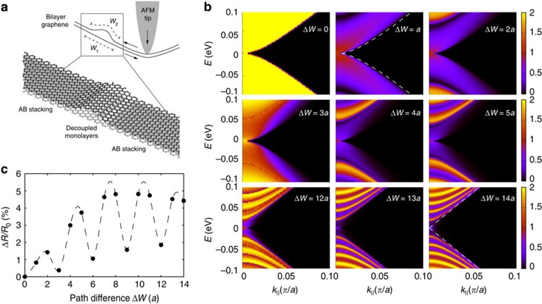
Figure 4. Theoretical simulations of charge-carrier transport.
(a) Schematic illustration of the lateral shift of individual graphene layers with respect to each other subjected to the AFM tip action. The AB-stacked bilayer graphene domains are separated by a region of decoupled monolayers of different effective width. (b) Calculated charge-carrier transmission probability across a region of decoupled graphene monolayers as a function of E and k|| for various charge-carrier path differences ΔW, given in units of lattice constant of graphene a. The dashed lines show the contours of the massive Dirac fermion band of bilayer graphene and the massless Dirac cone of monolayer graphene, respectively. (c) Relative electrical resistance ΔR/R0 of the simulated nanoelectromechanical device based on a bilayer GNR with a width of 50 nm under Vs=4 mV with a contact resistance Rc=41 kΩ as a function of charge-carrier path difference ΔW given in units of lattice constant of graphene a. The line is a guide to the eye.

