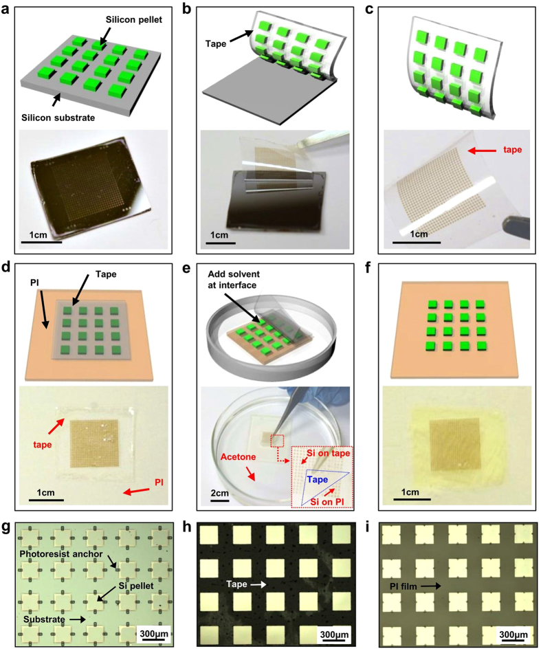
Figure 2. TTP operation procedure.
(a) Fabricated Si pellets array on an SOI wafer. (b) Picking up Si pellet array through peeling off the tape. (c) The high yield picked up Si pellet array on the tape. (d) Laminating the tape with Si pellet array facing the PI mediate and substrate. (e) Introducing acetone and peel off the tape from substrate. (f) The high yield printed Si pellet array on the PI. (g–i) Optical images of Si pellet array on SOI wafer, tape and PI, respectively. No variation of spatial configuration existed during the TTP operation procedure.

