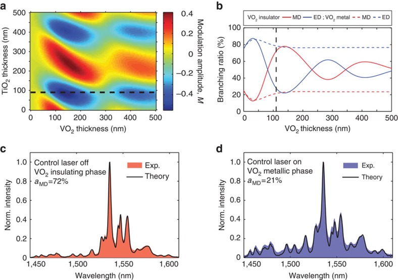
Figure 3. Device design and spectral modulation of Er3+ emission in multilayer structure.
(a) 2D colour plot of the calculated modulation amplitude of the MD contribution to Er3+ emission at 1.5 μm upon the VO2 phase-change, as a function of TiO2 and VO2 thicknesses. (b) Evolution of the branching ratio of ED (red) and MD (blue) emission as a function of the VO2 thickness (where  as indicated by the black line in a), before (solid lines) and after (dashed lines) inducing the VO2 insulator-to-metal transition. The black line labels the VO2 thickness used in our experiment. (c,d) Experimental and calculated spectra for Er3+ ions when VO2 is in the (c) insulating state and (d) metallic state. Experimental spectra are shown in shaded red and blue colour, respectively, whereas theoretically predicted spectra are shown as black solid lines. Exp, experimental; norm, normalized.

