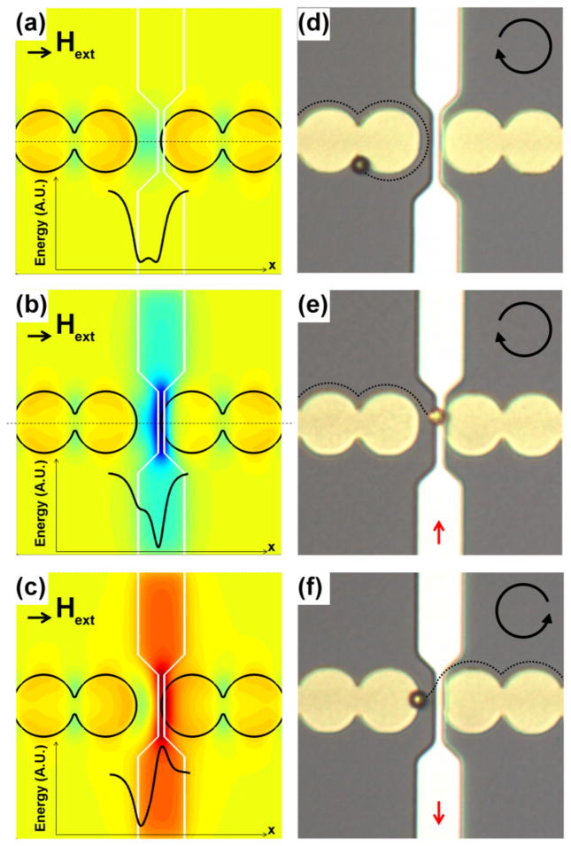
Figure 2. Transistor operational modes and their energy landscapes.
Magnetic potential energy landscapes are shown in (a–c) with corresponding experiments shown in (d–f). In (a–c), the line cross-sections are shown when no gate current is applied (a), in the attractive mode (b), and in the repulsive mode (c). In all cases, a constant uniform magnetic field is applied along the positive x-direction and denoted by the black arrow. In part (d), the bead remains on the same side of the gap due to the double well potential of part (a). In a clockwise rotating field (e), the bead moves across the gap towards the wire due to a gate current in the positive y-direction. In a counter-clockwise rotating field (f), the bead crosses the gap and moves away from the wire due to a gate current in the negative y-direction. Field rotation sense is denoted by the circular arrows, and gate currents are shown as red arrows.

