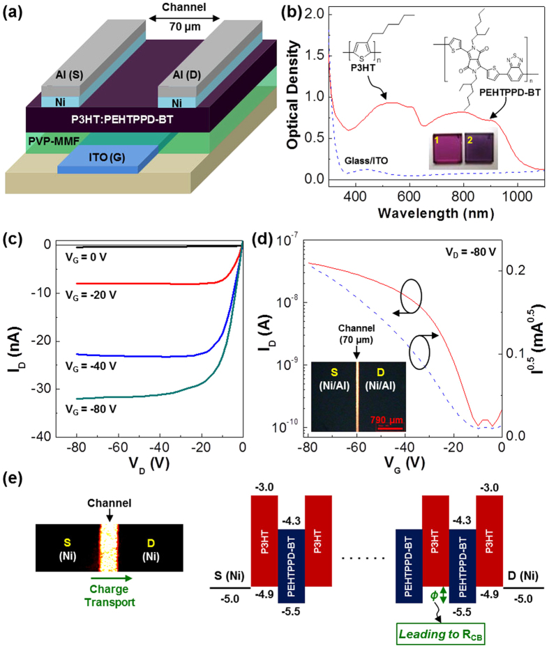
Figure 2. OPTR structure, broadband absorption and transistor performances.
(a) Device structure of OPTRs with all-polymer BHJ (P3HT:PEHTPPD-BT) layer. (b) Optical absorption spectra of the ITO-glass substrate and the P3HT:PEHTPPD-BT layer-coated ITO-glass substrate (see the photograph ‘2’ compared with the photograph ‘1’ of the P3HT layer-coated ITO-glass substrate). (c) Output characteristics of OPTR with the P3HT:PEHTPPD-BT layer in the dark. (d) Transfer characteristics of OPTR with the P3HT:PEHTPPD-BT layer in the dark (VD = −80 V): The inset optical microscope (OM) image shows the channel area for the OPTR fabricated in this work, where S and D denote the source electrode and the drain electrode, respectively. (e) Illustration for the charge blocking resistance (RCB) owing to the HOMO energy barrier (ϕ) (see the enlarged OM image on the left as a guide for charge transport direction).

