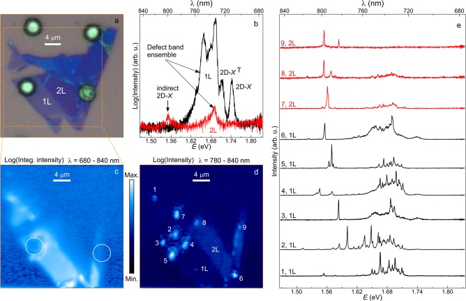
Figure 1.
(a) Optical micrograph of an exfoliated flake on top of a Si substrate with etched holes (1 μm deep, 4 μm diameter). (b) Typical PL emission spectra for 1L (black) and 2L (red) WSe2 from the smooth and unstrained locations of the flake. The ensemble emission due to defect-bound excitonic complexes can be seen in both 1L and 2L WSe2. (c–d) Color-coded spatial maps of PL with (c) integrated intensities in the spectral range of 680–840 nm and (d) intensities in the spectral range of 780–840 nm. (e) PL spectra corresponding to localized bright spots numbered in (d). The excitation power was 5 μW. The open square in (a) marks the region of spatial maps shown in (c) and (d). The two open circles in (c) mark the locations of the etched holes.

