
Fig. 4. Selective growth of perovskite crystals on prepatterned electrodes for photodetector arrays and FETs.
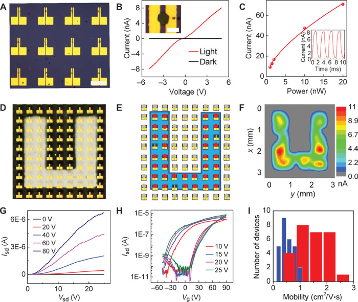
(A) Optical microscopy image of perovskite microplate crystals bridging prepatterned arrays of electrode pairs. Scale bar, 200 μm. (B) Typical I-V curve of a perovskite crystal under dark and light illumination. (Inset) Optical microscopy image of a perovskite crystal bridging two gold electrodes. The distance between the electrode pair is 8 μm. Scale bar, 20 μm. (C) Photocurrent versus incident light power of a typical device (source-drain voltage, 5 V). (Inset) Response speed of a typical two-probe device (laser illumination, 488 nm; power, 1.2 nW; source-drain voltage, 5 V). (D) Optical image of photodetector arrays with a U-shaped mask (U-shaped transparent area). (E) Schematic illustration of the device arrangement of photodetector arrays with a U-shaped mask under blue LED illumination (wavelength, 463 nm; power density, 600 μW/cm2). Red dots, devices with photocurrent; gray dots, devices without photocurrent. (F) Photocurrent mapping of photodetector arrays with a U-shaped mask under blue LED illumination. (G and H) Output (Vg = 0, 20, 40, 60, and 80 V) (G) and transfer (Vsd = 10, 15, 20, and 25 V) (H) characteristics of FET based on a perovskite microplate crystal at 77 K. (I) Distribution of the field effect electron mobility of 27 perovskite microplate transistors measured at 77 K. Red, mobility derived from backward sweep; blue, mobility derived from forward sweep.