
Fig. 1.
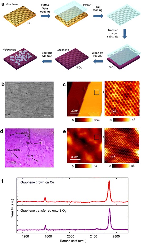
Preparation and characterization of graphene-coated samples. a Illustrative diagram showing PMMA-assisted transfer method used to obtain graphene-coated SiO2 substrates for present study, b SEM image of single layer graphene (SLG) grown on Cu sample, c large-scale STM topographic image (100 × 100 nm2) of SLG grown on Cu. The filtered atomically resolved image (3.5 × 3.5 nm2) shows the hexagonal lattice of SLG, d optical microscopy image of SLG transferred onto SiO2, e STM image of SLG transferred onto SiO2 displays honeycomb lattice and f representative Raman spectra Raman spectra of SLG grown on Cu (up) and SLG transferred onto SiO2 (down). Background caused by the luminescence of the copper was subtracted in the case of SLG grown and transferred onto Cu. Tunnel current and bias voltages for STM images were between 0.1 and 0.6 nA and 0.1–1 V respectively