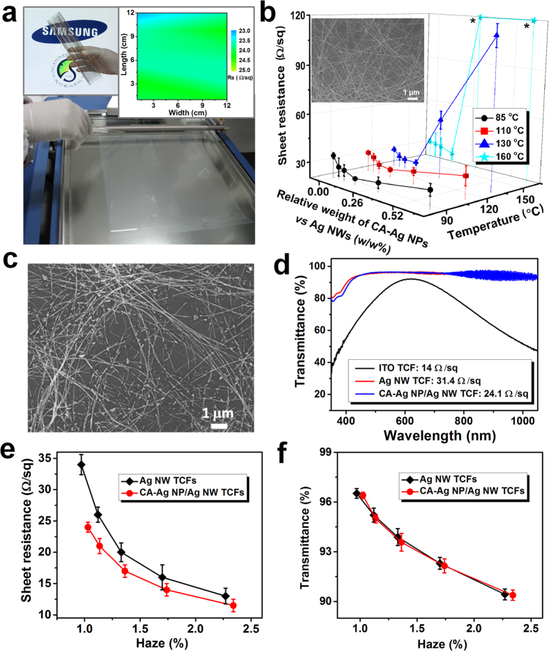
Figure 3. Electrical and optical properties of TCFs.
(a) Fabrication of CA-Ag NP/Ag NW TCFs on PC substrates (21 × 29.7 cm2). The inset images show the flexibility and area map for the sheet resistance of TCFs. The logos used in the figure were reproduced with permission from Samsung electronics and Sungkyunkwan University. (b) Sheet resistances of TCFs are shown as a function of the heat-treatment temperature and relative weight concentration of CA-Ag NPs and Ag NWs. The concentration of Ag NWs was fixed at 41.3 wt%. An SEM image of CA-Ag NP/Ag NW TCF cured at 85 °C (CA-Ag NP/Ag NW = 0.16 w/w%) is provided in the inset. (c) SEM image of CA-Ag NP/Ag NWs on a Si/SiO2 substrate. The relative concentration of CA-Ag NPs over Ag NWs was 0.16 w/w%, and the curing temperature was 160 °C. (d) Transmittance spectra of ITO, Ag NW, and CA-Ag NP/Ag NW TCFs. (e,f) Sheet resistance and total transmittance of Ag NW and CA-Ag NP/Ag NW TCFs are shown as a function of the haze. The Ag NW concentration was varied from 41.3 to 70.6 wt%. The relative concentration of CA-Ag NPs over Ag NWs was fixed at 0.16 w/w% for CA-Ag NP/Ag NWs. The curing temperature was 85 °C.

