Abstract
We present a microscopic study on the impact of doping on the carrier dynamics in graphene, in particular focusing on its influence on the technologically relevant carrier multiplication in realistic, doped graphene samples. Treating the time- and momentum-resolved carrier-light, carrier-carrier, and carrier-phonon interactions on the same microscopic footing, the appearance of Auger-induced carrier multiplication up to a Fermi level of 300 meV is revealed. Furthermore, we show that doping favors the so-called hot carrier multiplication occurring within one band. Our results are directly compared to recent time-resolved ARPES measurements and exhibit an excellent agreement on the temporal evolution of the hot carrier multiplication for n- and p-doped graphene. The gained insights shed light on the ultrafast carrier dynamics in realistic, doped graphene samples.
A number of theoretical and experimental studies has been performed aiming at a thorough understanding of the carrier relaxation dynamics in optically excited graphene1,2,3,4,5,6,7,8,9,10,11,12,13,14,15. Most of these studies focus on the ultrafast Coulomb- and phonon-induced carrier dynamics without considering the influence of doping in the investigated graphene samples. A non-zero Fermi level can have a crucial impact on the relaxation dynamics via a significant increase of the scattering phase space and via the enhancement of Pauli blocking. A first experimental time-resolved ARPES study has been performed addressing the doping dependence of carrier multiplication of graphene16. The underlying elementary processes determining the observed different behavior for p- and n-doped samples have not been microscopically investigated, yet.
In this work, we apply a microscopic approach to access the time-, momentum-, and angle-resolved dynamics of electrons and phonons in optically excited graphene under the influence of a variable n- and p-doping. The focus lies in particular on the impact of a finite Fermi level on the appearance of the technologically relevant carrier multiplication16,17,18,19,20,21,22,23,24,25,26,27. This interesting ultrafast phenomenon is related to the linear electronic band structure of graphene opening up the possibility of efficient Coulomb-induced Auger processes. A significant multiple carrier generation has been theoretically predicted17,19,26 and experimentally confirmed in graphene16,21,22,25,27. So far, the theoretical studies have been constrained to the case of undoped graphene. Introducing a non-zero Fermi level in graphene, electrons above the Dirac point or above the Fermi level can be considered as charge carriers (holes in analogy). In the first case, the carrier multiplication can take place via Auger scattering bridging the valence and the conduction band. In the following, we label this process as carrier multiplication (CM). On the other side, counting carriers with respect to the Fermi level, the multiplication occurs via Coulomb-induced intraband scattering bridging the states below and above the Fermi level, cf. Fig. 1. According to literature21, we label this process as hot carrier multiplication (hCM). Here, the actual number of charge carriers remains unchanged in each band. Nevertheless, since these hot carriers are crucial for many technological applications, the appearance of hCM is also of technological relevance.
Figure 1. Schematic illustration of Coulomb-induced scattering processes for optically excited n-doped graphene.
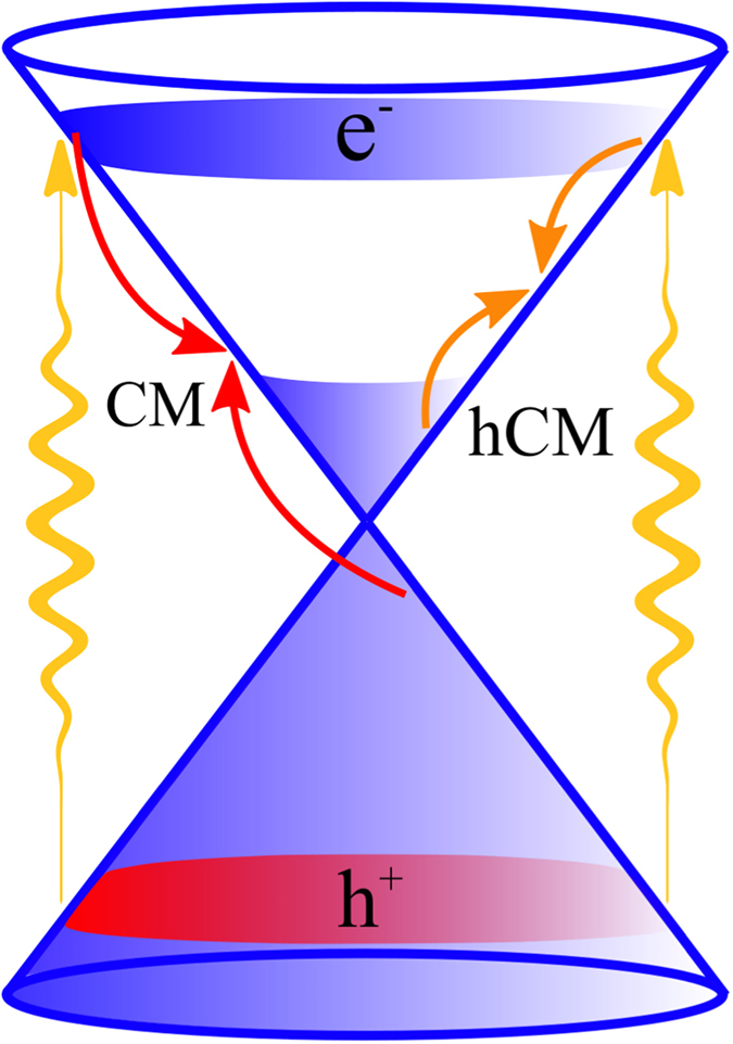
In the presence of a finite Fermi level, carrier multiplication (CM) and hot carrier multiplication (hCM) need to be distinguished. While the first is induced by Auger processes bridging the valence and the conduction band (red arrows) and increasing the number of charge carriers in the conduction band, the second corresponds to Coulomb-induced intraband scattering (orange arrows) and increases the number of carriers above the Fermi level.
Theoretical approach
The starting point for the calculation is the many-particle Hamilton operator H = H0 + Hc,f + Hc,p + Hc,c, where H0 denotes the interaction-free carrier and phonon part, Hc,l the carrier-light coupling, Hc,p the carrier-phonon interaction, and Hc,c the carrier-carrier interaction28. The carrier dynamics is described by graphene Bloch equations1 corresponding to a coupled set of differential equations for the occupation probability  in the state k and the band λ = (v, c), the microscopic polarization pk(t) that is a measure for the optical transition probability between both bands, and the phonon occupation
  with the momentum q for different optical and acoustic phonon modes j29:
 |
 |
 |
Here,  is the optical transition frequency within the linear electronic band structure
  of graphene close to the Dirac point. The carrier-light coupling is determined by
  with the optical matrix element29
 , the vector potential A(t) representing the excitation pulse, the free electron mass m0, and the charge e0. Here,
  is the Rabi frequency and
  accounts for intraband transitions12. The many-particle interactions are treated within the second-order Born-Markov approximation1,28,30,31, which yields a Boltzmann-like scattering equation for the carrier occupation with the time- and momentum-dependent scattering rates
  accounting for Coulomb- and phonon-induced processes. At the same time, the microscopic polarization is damped by the many-particle-induced diagonal dephasing γk(t) and is driven by the off-diagonal dephasing term Uk(t). In analogy, the equation of motion for the phonon occupation
  is obtained and contains phonon emission and absorption rates
  . The finite phonon lifetime32
γph is considered by a coupling to a phonon bath
  at room temperature. The explicit form of the time- and momentum-dependent scattering rates is discussed in the supplementary material. More details on the diagonal and off-diagonal dephasing terms can be found in Malic et al.29.
A finite Fermi level EF breaks the symmetry between the valence and conduction band around the Dirac point, cp. Fig. 1. As a result, the occupation probability of electrons  and of holes
  needs to be treated separately. As initial condition, we assume a Fermi distribution
  where + stands for the hole and − for the electron occupation at the temperature T. Another important aspect of doping is the increased screening of the Coulomb interaction. The bare Coulomb potential Vq appearing in the Coulomb-induced scattering rates
  is screened via the dynamic dielectric function ε(q, ω) that is defined by the Lindhard equation28,33, cf. the supplementary material for a more detailed discussion. Since this many-particle-induced screening is directly influenced by carrier occupations in the conduction and valence bands, doping plays a crucial role and has a significant influence on the ultrafast carrier dynamics in graphene.
With the presented microscopic approach, we can track the relaxation dynamics of non-equilibrium charge carriers in time, and energy including the temporal evolution of the carrier density after the optical excitation. First, we focus on the electron and hole dynamics in highly doped graphene and then we discuss the impact of doping on the appearance of carrier multiplication.
Results and Discussion
Electron and hole dynamics
Here, we discuss how the doping-induced symmetry breaking between electrons in the conduction band and holes in the valence band influences the dynamics of optically excited charge carriers in realistic doped graphene samples. Figure 2 illustrates the angle-averaged occupation probability  for (a) electrons and (b) holes for an initial Fermi level of 300 meV as a function of the carrier energy for different times after the optical excitation. Note that for symmetry reasons, the physical picture remains the same in p-doped graphene samples but electrons and holes switch their roles, respectively. The system is excited by a 10 fs pulse with a photon energy of 1.5eV and a pump fluence of 0.3 μJcm−2. The characteristics of the excitation pulse correspond to typical values that can be realized by standard pulsed lasers34. The pulse is centered at 0fs and gives rise to a well pronounced non-equilibrium distribution for electrons and holes around the carrier energy of 0.75eV, cf. Fig. 2. For both electrons and holes, the efficient carrier-carrier and carrier-phonon scattering leads to an ultrafast thermalization of the system towards a hot Fermi distribution already after some tens of femtoseconds. Then, a slower phonon-induced carrier cooling occurs that drives the electron and hole occupations towards their initial thermal Fermi distributions. Due to the increased number of available scattering partners in the conduction band of n-doped graphene, the Coulomb-driven carrier thermalization occurs faster for electrons. Here, a hot thermalized Fermi distribution is already reached after 30 fs, while at the same time the holes exhibit still a non-equilibrium distribution, cf. the purple lines in Fig. 2.
Figure 2. Electron and hole occupations in doped graphene.
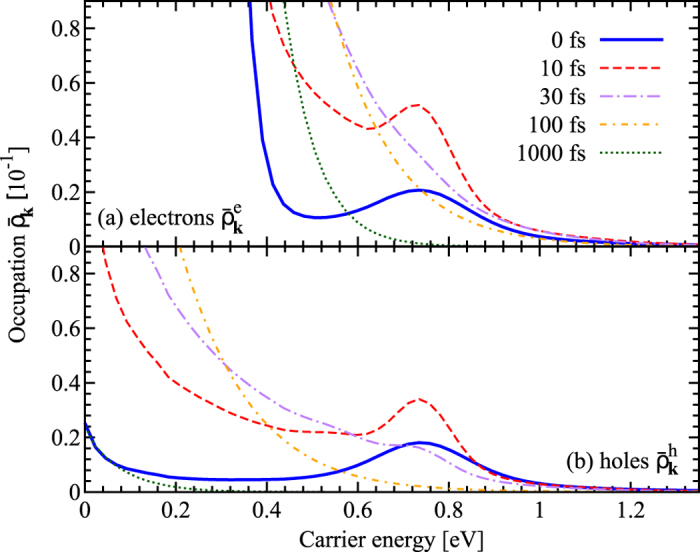
Angle-averaged occupation probability  for (a) electrons and (b) holes in highly n-doped graphene (EF = 300 meV) is shown as a function of the carrier energy for different times after the optical excitation. Note that due to the n-doping the electron relaxation is faster resulting in a thermalized hot Fermi distribution already after 30 fs. The inverse behavior can be found for p-doped graphene.
Carrier multiplication (CM)
Now, we study the impact of an initial Fermi level EF on the Coulomb-induced multiple carrier generation, which is generally defined as the ratio between the number of overall generated electron-hole pairs and the optically excited charge carriers
 |
where n is the total carrier density, nT the initial thermal carrier background, and nopt the optically excited carrier density. All contributions contain both electrons in the conduction band as well as holes in the valence band. For doped graphene, the specific definition depends on the physical situation: For optical measurements probing vertical carrier transitions, a definition with respect to to the Dirac point is reasonable, i.e.  and
and  . The carrier density then reads
 |
where L2 is the graphene area and σs (σv) denotes the spin (valley) degeneracy. On the other side, electric transport phenomena are also of great interest, where hot electrons around the Fermi level are relevant giving rise to a hot carrier multiplication, cf. Fig. 1. This situation will be discussed in the next section.
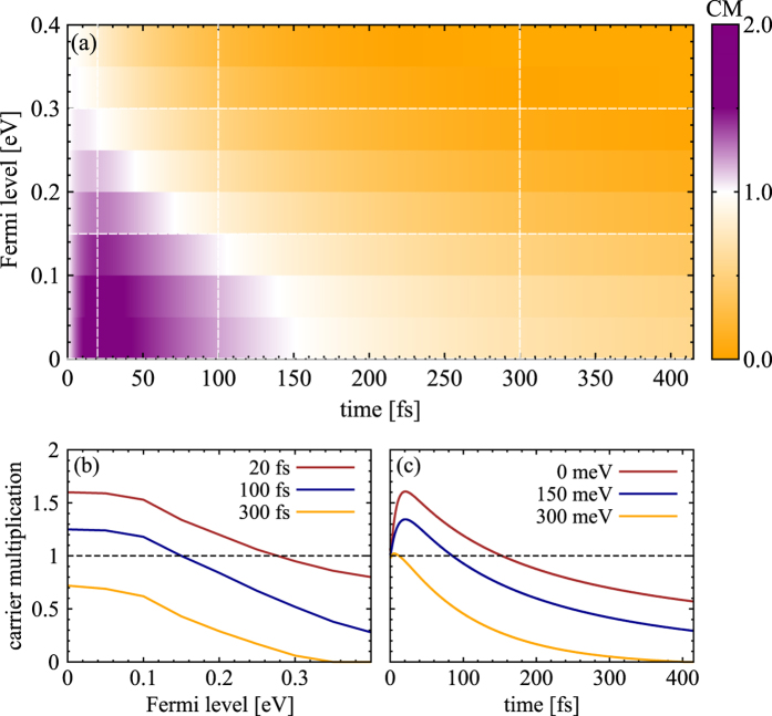
Treating the full set of graphene Bloch equations, we have microscopic access to the temporal evolution of the carrier density including the contributions of carrier-light, carrier-carrier, and carrier-phonon interactions. Figure 3(a) illustrates the temporal evolution of CM as a function of the initial Fermi level EF at a fixed absorbed pump fluence of 0.3 μJcm−2. The surface plot reveals that doping clearly reduces the CM efficiency: The lower EF, the higher is the CM factor reaching values of up to approximately 1.7 for undoped graphene at the considered pump fluence, cf. Fig. 3(b). CM can be observed for EF of up to 300 meV. It occurs on a timescale of up to 150 fs for undoped graphene and becomes significantly shorter for increasing doping, as illustrated in Fig. 3(c). The observed CM in the low-doping case can be explained by the strongly efficient impact excitation (IE) prevailing over the inverse process of Auger recombination (AR), which is a result of the large gradient in carrier occupation around the Dirac point, cf. Fig. 2(a). For undoped graphene, the probability for IE can be written as ρv(1 − ρc) ≈ 1, whereas the probability for AR is given by ρc(1 − ρv) ≈ 0 (since ρv ≈ 1 and ρc ≈ 0). In this case, IE is significantly favored by Pauli blocking during the initial dynamics. This is reflected by the corresponding rates γIE and γAR that are shown in Fig. 4(a). We observe that the IE rate is clearly higher for a time range of approximately 100 fs determining the strength of the appearing CM. During the carrier relaxation both rates converge to the same value and end up in an equilibrium, where no more carriers are generated. The timescale of the CM is determined by the duration of the imbalance between IE and AR rates in combination with the interplay with competing channels of carrier-phonon scattering, which transfer energy from the electronic system to the lattice. With an increasing doping, Auger scattering becomes more and more Pauli blocked resulting in overall lower rates, cf. Fig. 4(b). For Fermi levels higher than 300 meV, AR becomes the dominant relaxation channels and CM does not appear anymore.
Figure 3. Doping dependence of carrier multiplication (CM).
(a) Temporal evolution of the doping-dependent CM for a fixed absorbed pump fluence of εabs = 0.3 μJcm−2 and an excitation energy of 1.5 eV. (b) CM as a function of the Fermi level EF for three fixed time delays and (c) the temporal evolution of CM for three fixed Fermi levels. Note that CM only takes place for EF smaller than 0.3eV and for times up to 150 fs. (purple area in part (a)).
Figure 4. Auger rates in doped graphene.
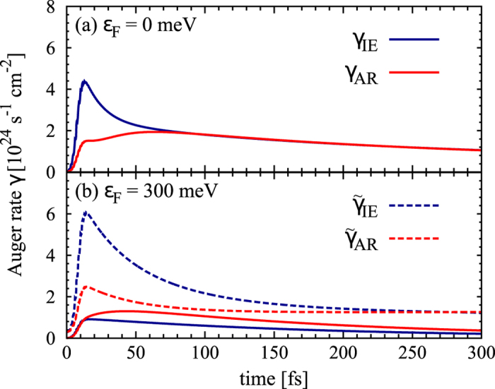
Temporal evolution of Auger rates including impact excitation (IE) and the inverse process of Auger recombination (AR) for (a) undoped and (b) highly n-doped graphene (ε = 300 meV). In the latter case, also the corresponding intraband Auger rates ( ,
,  ) describing Coulomb-induced scattering bridging the states below and above the Fermi level are illustrated (dashed lines), cf. Fig. 1. In undoped graphene, there is a clear asymmetry between both Auger processes in favor of IE in the first 100 fs. In the doped case, γAR is significantly larger than γIE, however, for intraband Auger rates, the situation is opposite and
  clearly prevails over
  resulting in a pronounced hot carrier multiplication.
Hot carrier multiplication (hCM)
Now, we focus on the situation, where charge carriers are defined with respect to the Fermi level, i.e. for n-doped graphene the upper Dirac cone is split into  for k > kF and
  for k < kF with the Fermi momentum kF. The bottom cone remains unaffected with
  . The according hot carrier density
  is given by
 |
and the associated hot carrier multiplication is highly relevant for transport phenomena16,21, cf. Fig. 1. Note that we obtain symmetric results for n- and p-doped graphene, since the contribution of both electrons and holes to the carrier density is considered. For undoped graphene, both definitions of carrier density [Eqs. (5) and (6)] and carrier multiplication are equivalent for symmetry reasons.
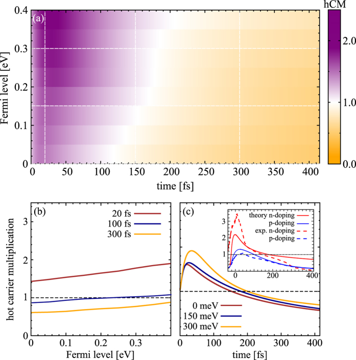
The surface plot in Fig. 5(a) illustrates hCM as a function of the Fermi level EF and time at a fixed absorbed pump fluence of εabs = 0.3 μJcm−2. In contrast to the behavior of CM, we observe a clear increase of hCM with doping. We reach hCM factors of up to approximately 2 (at the considered pump fluence) on a timescale of about 200 fs for highly doped graphene with EF = 300 meV, cf. Fig. 5(b,c). There is nearly a linear dependence between hCM and doping: The smaller EF, the less pronounced is hCM, and the faster it decays. The probability for intraband IE processes is given by ρh,c(1 − ρe,c), which is initially large compared to the probability for intraband AR processes ρe,c(1 − ρh,c), cf. Fig. 1. With the increasing Fermi level, the intraband Auger processes are shifted into a region of higher density of states making them more efficient, as reflected by the much higher scattering rates displayed in Fig. 4(b). The initial strong imbalance between  and
and  gives rise to a pronounced hCM.
Figure 5. Doping dependence of hot carrier multiplication (hCM).
The same plot as in Fig. 4 illustrating now the temporal evolution of the doping-dependent hCM for a fixed absorbed pump fluence of εabs = 0.3 μJcm−2. The inset in (c) shows a direct comparison between theoretically predicted (solid lines) and experimentally measured time-resolved ARPES data (dashed lines) for: (i) n-doped graphene (EF = 380 meV, εabs = 0.5 μJcm−2) and (ii) p-doped graphene (EF = 240 meV, εabs = 1.5 μJcm−2). The experimental data is taken from Johannsen et al.16.
Besides the discussed doping dependence, CM or hCM are strongly sensitive to the excitation regime. A detailed discussion is provided in the supplementary material, where a semi-analytical approach is presented focusing on the purely Coulomb-induced CM and hCM.
Direct comparison to experimental data
After having presented the theoretical results on the doping dependence of the carrier multiplication, we perform a direct comparison with recently performed time-resolved ARPES measurements on n- and p-doped graphene samples16. We explicitly take into account the experimental conditions, such as the Fermi level and the excitation strength. Considering that our microscopic theory does not contain any fitting parameters, we obtain an excellent agreement between theory and experiment, cf. the inset in Fig. 5(c). There is a clearly higher hCM for n-doped graphene reaching values of up to 2.2 in the theory and more than 3 in the experiment. In contrast, for p-doped graphene only a small hCM of 1.4 or 1.2 is obtained in theory and experiment, respectively. This pronounced difference is not due to the type of doping (n, p), as one might assume16. It can be clearly explained by the differences in the applied fluence εabs and the actual Fermi level EF. Note that at the exactly same conditions with respect to EF and εabs, we obtain the same hot carrier multiplication for both n- and p-doped samples. However, the experiment has been performed for: (i) n-doped graphene with the Fermi level EF = 380 meV and an absorbed pump fluence of εabs = 0.5 μJcm−2 and (ii) p-doped graphene with EF = 240 meV and εabs = 1.5 μJcm−2. As shown in Fig. 5(b), hot carrier multiplication increases almost linearly with the Fermi level. Furthermore, it is strongly suppressed in the strong excitation regime, i.e. the larger the pump fluence, the less efficient is the hCM, as illustrated in Fig. S3 in the supplementary material. As a result, the n-doped graphene sample shows a much more pronounced hCM, since its Fermi level EF is significantly higher and since the experiment has been performed at a clearly smaller pump fluence compared to the p-doped graphene sample. While the theory qualitatively reproduces well the experimental data, quantitatively, it underestimates the CM value in the first 50 fs as well as its temporal decay in the n-doped case. This might be due to the applied semi-Markovian description of the CM processes1. A full non-Markovian approach would allow for a dynamical build-up of the screening of the Coulomb interaction and would lead to more allowed scattering channels on short time scales. Another possible reason for the deviation in the first 50 fs is that the experimental estimate of the carrier density is based on the introduction of a carrier temperature. However, the latter can only be well defined once a thermalized carrier distribution is reached, which occurs during that timescale. The faster temporal decay of the CM in the experiment could also be explained by the occurrence of additional scattering channels in a non-Markovian description or might suggest an additional impurity-induced scattering channel that accelerates the CM decrease.
In conclusion, we have presented a microscopic study of the carrier dynamics in doped graphene samples, in particular focusing on the impact of a finite Fermi level on the (hot) carrier multiplication. We reveal the appearance of Auger-induced carrier multiplication up to Fermi levels of 300 meV. In the case of the hot carrier multiplication occurring within one band doping is even advantageous, since it increases the phase space by providing a large number of available scattering partners. Finally, we have directly compared our results to recent time-resolved ARPES measurements finding an excellent agreement and providing a microscopic explanation for the observed different behavior in n- and p-doped graphene samples. Our results contribute to a better understanding of the ultrafast carrier dynamics in realistic graphene samples and give valuable insights into the technologically relevant carrier multiplication in graphene.
Additional Information
How to cite this article: Kadi, F. et al. Impact of doping on the carrier dynamics in graphene. Sci. Rep. 5, 16841; doi: 10.1038/srep16841 (2015).
Supplementary Material
Acknowledgments
We acknowledge financial support from the Deutsche Forschungsgemeinschaft (DFG) through SPP 1458 (T.W. and E. M.), SFB 658 (F.K.) and SFB 951 (A.K.). Furthermore, E.M. is thankful to the EU Graphene Flagship (CNECT-ICT-604391) and the Swedish Research Council (VR).
Footnotes
Author Contributions F.K. performed the calculations and wrote the paper with major input from E.M., T.W., A.K. and E.M. analysed and discussed the results.
References
- Malic E. & Knorr. A. Graphene and Carbon Nanotubes: Ultrafast Optics and Relaxation Dynamics (Wiley-VCH, 2013). [Google Scholar]
- Dawlaty J. M., Shivaraman S., Chandrashekhar M., Rana F. & Spencer M. G.. Measurement of ultrafast carrier dynamics in epitaxial graphene. Appl. Phys. Lett. 92, 042116–042116-3 (2008). [DOI] [PubMed] [Google Scholar]
- Plochocka P. et al. Slowing hot-carrier relaxation in graphene using a magnetic field. Phys. Rev. B 80, 245415 (2009). [Google Scholar]
- Wang H. et al. Ultrafast relaxation dynamics of hot optical phonons in graphene. Appl. Phys. Lett. 96, 081917 (2010). [Google Scholar]
- Obraztsov P. A. et al. Broadband light-induced absorbance change in multilayer graphene. Nano Lett. 11, 1540–1545 (2011). [DOI] [PubMed] [Google Scholar]
- Winnerl S. et al. Carrier relaxation in epitaxial graphene photoexcited near the dirac point. Phys. Rev. Lett. 107, 237401 (2011). [DOI] [PubMed] [Google Scholar]
- Sun D. et al. Current relaxation due to hot carrier scattering in graphene. New J. Phys. 14, 105012 (2012). [Google Scholar]
- Malard L. M., Mak K. F., Neto A. H. C., Peres N. M. R. & Heinz T. F.. Observation of intra- and inter-band transitions in the transient optical response of graphene. New J. Phys. 15, 015009 (2013). [Google Scholar]
- Johannsen J. C. et al. Direct view of hot carrier dynamics in graphene. Phys. Rev. Lett. 111, 027403 (2013). [DOI] [PubMed] [Google Scholar]
- Gierz I. et al. Snapshots of non-equilibrium dirac carrier distributions in graphene. Nature Mater. 12, 1119–1124 (2013). [DOI] [PubMed] [Google Scholar]
- Tomadin A., Brida D., Cerullo G., Ferrari A. C. & Polini M.. Nonequilibrium dynamics of photoexcited electrons in graphene: Collinear scattering, auger processes, and the impact of screening. Phys. Rev. B 88, 035430 (2013). [Google Scholar]
- Kadi F. et al. Microscopic description of intraband absorption in graphene: The occurrence of transient negative differential transmission. Phys. Rev. Lett. 113, 035502 (2014). [DOI] [PubMed] [Google Scholar]
- Mittendorff M. et al. Anisotropy of excitation and relaxation of photogenerated charge carriers in graphene. Nano Lett. 14, 1504–1507 (2014). [DOI] [PubMed] [Google Scholar]
- Winzer T. et al. Microscopic view on the ultrafast photoluminescence from photo-excited graphene. Nano Lett. 15, 1141 (2015). [DOI] [PubMed] [Google Scholar]
- Mittendorff M. et al. Carrier dynamics in landau-quantized graphene featuring strong auger scattering. Nature Phys. 11, 75 (2015). [Google Scholar]
- Johannsen J. C. et al. Tunable carrier multiplication and cooling in graphene. Nano Lett. 15, 326–331 (2015). [DOI] [PubMed] [Google Scholar]
- Winzer T., Knorr A. & Malic E.. Carrier multiplication in graphene. Nano Lett. 10, 4839–4843 (2010). [DOI] [PubMed] [Google Scholar]
- Song J. C. W., Rudner M. S., Marcus C. M. & Levitov L. S.. Hot carrier transport and photocurrent response in graphene. Nano Lett. 11, 4688–4692 (2011). [DOI] [PubMed] [Google Scholar]
- Winzer T. & Malić E.. Impact of auger processes on carrier dynamics in graphene. Phys. Rev. B 85, 241404 (2012). [Google Scholar]
- Pirro L., Girdhar A., Leblebici Y. & Leburton J.-P.. Impact ionization and carrier multiplication in graphene. J. Appl. Phys. 112, 093707 (2012). [Google Scholar]
- Tielrooij K. J. et al. Photoexcitation cascade and multiple hot-carrier generation in graphene. Nature Phys. 9, 248 (2013). [Google Scholar]
- Brida D. et al. Ultrafast collinear scattering and carrier multiplication in graphene. Nature Commun. 4, 1987 (2013). [DOI] [PubMed] [Google Scholar]
- Song J. C. W., Tielrooij K. J., Koppens F. H. L. & Levitov L. S.. Photoexcited carrier dynamics and impact-excitation cascade in graphene. Phys. Rev. B 87, 155429 (2013). [Google Scholar]
- Basko D. M.. Effect of anisotropic band curvature on carrier multiplication in graphene. Phys. Rev. B 87, 165437 (2013). [Google Scholar]
- Plötzing T. et al. Experimental verification of carrier multiplication in graphene. Nano Lett. 14, 5371 (2014). [DOI] [PubMed] [Google Scholar]
- Wendler F., Knorr A. & Malic E.. Carrier multiplication in graphene under landau quantization. Nature Commun. 5, 3703 (2014). [DOI] [PubMed] [Google Scholar]
- Gierz I. et al. Tracking primary thermalization events in graphene with photoemission at extreme timescales. Phys. Rev. Lett. 115, 086803 (2015). [DOI] [PubMed] [Google Scholar]
- Haug H. & Koch. S. W. Quantum Theory of the Optical and Electronic Properties of Semiconductors (World Scientific, 2004). [Google Scholar]
- Malic E., Winzer T., Bobkin E. & Knorr A.. Microscopic theory of absorption and ultrafast many-particle kinetics in graphene. Phys. Rev. B 84, 205406 (2011). [Google Scholar]
- Knorr A., Hughes S., Stroucken T. & Koch S.. Theory of ultrafast spatio-temporal dynamics in semiconductor heterostructures. Chem. Phys. 210, 27–47 (1996). [Google Scholar]
- Kira M. & Koch S. W.. Semiconductor Quantum Optics (Cambridge University Press, 2011). [Google Scholar]
- Kang K., Abdula D., Cahill D. G. & Shim M.. Lifetimes of optical phonons in graphene and graphite by time-resolved incoherent anti-stokes raman scattering. Phys. Rev. B 81, 165405 (2010). [Google Scholar]
- Guiliani G. & Vignale G.. Quantum Theory of the Electron Liquid (Cambridge University Press, 2005). [Google Scholar]
- Breusing M. et al. Ultrafast nonequilibrium carrier dynamics in a single graphene layer. Phys. Rev. B 83, 153410 (2011). [Google Scholar]
Associated Data
This section collects any data citations, data availability statements, or supplementary materials included in this article.


