Abstract
We report a novel concept of graphene transistors on Scotch tape for use in ubiquitous electronic systems. Unlike common plastic substrates such as polyimide and polyethylene terephthalate, the Scotch tape substrate is easily attached onto various objects such as banknotes, curved surfaces, and human skin, which implies potential applications wherein electronics can be placed in any desired position. Furthermore, the soft Scotch tape serves as an attractive substrate for flexible/foldable electronics that can be significantly bent, or even crumpled. We found that the adhesive layer of the tape with a relatively low shear modulus relaxes the strain when subjected to bending. The capacitance of the gate dielectric made of oxidized aluminum oxide was 1.5 μF cm−2, so that a supply voltage of only 2.5 V was sufficient to operate the devices. As-fabricated graphene transistors on Scotch tape exhibited high electron mobility of 1326 (±155) cm2 V−1 s−1; the transistors still showed high mobility of 1254 (±478) cm2 V−1 s−1 even after they were crumpled.
Recent advances in flexible device technology have changed the paradigm of electronics from rigid objects to flexible form factors1. Flexible displays2, sensors3,4, circuits5,6, solar cells7, and batteries8 have become popular subjects in both academia and industry, and such components have facilitated the development of bendable consumer products. One of the most popular approaches for making flexible devices is to use flexible plastic substrates, such as polyimide and polyethylene terephthalate, and to fabricate electronic components on them at a low temperature at which substrate deformation does not occur9. Alternatively, flexible and conformable substrates such as polydimethylsiloxane and a commercial tattoo can also be used on which a thin layer of electronic devices is laminated5,10. Flexible devices can also be directly prepared onto nonconventional substrates including banknotes and papers11,12,13. These methods have gradually expanded the use of electronics.
In this study, we developed a method for flexible and conformable electronic devices on Scotch tape. Scotch tape, which serves as a remarkably flexible substrate, is simply attached on various objects as long as the adhesive of the tape adheres; as a result, Scotch tape electronics can be utilized to accomplish ubiquitous electronic systems for applications of interest. Another advantage of such a Scotch tape substrate is that the adhesive layer of the tape relaxes the strain when subjected to bending. We analyzed the mechanical strain applied to a bent Scotch tape substrate. Because of its soft layers, transistors on top of the Scotch tape, i.e., non-adhesive side, experience a significantly lower tensile strain as compared to regular polyimide under the same bending condition. We used graphene as the channel material. Graphene is not only one of the most representative flexible electronic materials14,15, but also a promising candidate for signal conditioning in electronics16,17. In particular, graphene devices are widely studied for the radio-frequency technology, which enables wireless communication18,19. Thus, the fabrication of graphene transistors on Scotch tape would be a significant step toward realizing ubiquitous electronics.
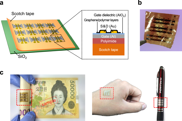
The device structure is shown in Fig. 1. Graphene field-effect transistors (GFETs) were fabricated on Scotch tape attached on a silicon dioxide (SiO2) wafer (Fig. 1a). After fabrication, the Scotch tape substrate was peeled off from the wafer and ready to be placed onto various nonconventional surfaces (Fig. 1b). As shown in Fig. 1c, the GFETs on the Scotch tape were easily attached on a banknote, human skin, and a pen without any adverse effects on the electrical properties. Scotch tape as a substrate is superior to widely used polyimide for flexible/foldable electronics; the Young’s modulus of the Scotch tape in this study is approximately 0.4 GPa as compared to 2.5 GPa for polyimide20. However, Scotch tape exhibits a lower operating temperature, less chemical resistance, and more outgassing in a vacuum chamber than polyimide, thereby requiring mild fabrication procedures to prevent any defects in the delicate substrate.
Figure 1. Device structure and its applications.
(a) Schematic of device structure. The Scotch tape substrate was attached on a silicon dioxide (SiO2) wafer during fabrication. (b) After device fabrication, the Scotch tape substrate was easily peeled off from the wafer. (c) The Scotch tape device was then attached on nonconventional objects such as banknote (W 50,000 Korean won), human skin, and pen (Copyright 2013 Pohang University of Science and Technology).
The gate dielectric is one of the most important components in field-effect transistors (FETs). Especially, high capacitance with a low leakage current is essential for low-power electronic devices that can be operated by portable batteries. Several methods have been used to meet the dielectric requirements for flexible transistors: atomic layer deposition (ALD) of aluminum oxide (AlOX)21,22, ion-gel dielectrics23,24, and oxidation of aluminum thin films25. Among these approaches, the oxidation of aluminum thin films with oxygen plasma, which does not require high temperature, solvent, or high-purity gas, is a feasible process for a Scotch tape substrate. Previously, oxygen plasma treatment on aluminum was demonstrated to form a high-capacitance AlOX gate dielectric for flexible organic transistors; however, an additional self-assembled monolayer (SAM) prepared by soaking in a solution was required on AlOX or else the leakage current through the dielectric increased significantly25. As solution-processed SAMs are not suitable for Scotch tape substrates, we improved the fabrication process for oxidized AlOX by optimizing the plasma conditions so that a single AlOX layer could be used as the gate dielectric for GFETs.
In a plasma system, the amount and movement of plasma particles are affected by power and pressure26. In particular, the kinetic energy of plasma ions is related to pressure, as shown in Equation 1, which describes the mean free path of a gaseous particle
 |
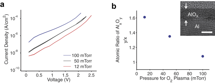
where k is the Boltzmann constant, T is the temperature, d is the collision diameter of the molecule, and P is the pressure. Therefore, oxygen radicals can penetrate the aluminum surface more effectively with a higher kinetic energy under lower pressure. We oxidized the surface of aluminum thin film (30 nm) deposited on a SiO2 wafer in an oxygen plasma chamber for 7 min. During plasma treatment, three different oxygen pressure values were used: 12, 50, and 100 mTorr. The electrical properties of the oxidized AlOX were tested after the deposition of the gold top electrode. The AlOX samples prepared using different oxygen pressures had an almost identical capacitance of 1.5 (±0.1) μF cm−2, which is equivalent to the capacitance of 2.3-nm-thick SiO2. However, there was a considerable difference in the leakage current of the three AlOX samples. As the oxygen pressure for plasma treatment decreased, the leakage current through the AlOX layer decreased, and the breakdown voltage increased (Fig. 2a). These results indicate that lower oxygen pressure facilitates a denser oxide film with better quality. Because of the large capacitance, only 1–1.5 V is sufficient to operate FETs by using the plasma-treated AlOX as the gate dielectric. In a previous study in which the ALD of AlOX with a SAM was employed27, the capacitance of the gate dielectric (total thickness of 6.4 nm) was approximately 0.5 μF cm−2, and its leakage current was on the order of 10−7 A cm−2 at 3 V. Applying 3 V to the 0.5 μF cm−2 capacitor induces an amount of charges equal to that from our 1.5 μF cm−2 AlOX capacitor with only 1 V. In Fig. 2a, the gate leakage current through AlOX (12 mTorr oxygen) at 1 V is on the order of 10−8 A cm−2, an order of magnitude lower than that in the previous study. We performed X-ray photoelectron spectroscopy (XPS) on the AlOX samples to investigate their chemical composition. The inelastic mean free path of electrons in AlOX is less than 5 nm at 1420 eV—the maximum electron kinetic energy in this XPS measurement28. Therefore, the angle between the photoelectron detector and the sample stage was tilted by 80° to ensure that all of the measured photoelectrons came from AlOX. The atomic ratio of AlOX as a function of oxygen pressure is shown in Fig. 2b; lower oxygen pressure during the plasma resulted in a higher relative ratio of oxygen. (Note that the oxygen ratio was overestimated to some degree because oxygen and water molecules adsorbed on the AlOX surface cannot be completely removed even under high-vacuum conditions.) Thus, the insulating property of AlOX is improved with the increase in the oxygen ratio. The thickness of AlOX fabricated at an oxygen pressure of 12 mTorr was measured to be 5.7 nm by transmission electron spectroscopy (TEM), as shown in the inset of Fig. 2b. By assuming a dielectric constant of 9.5 for the AlOX layer, the measured thickness is in good agreement with the capacitance value above.
Figure 2. Analysis on oxidized aluminum (AlOX) thin film.
(a) Leakage current of AlOX under different pressure conditions during plasma treatment. As the pressure decreased, the leakage current through AlOX was reduced, and the breakdown voltage increased. (b) X-ray photoelectron spectroscopy (XPS) data of AlOX prepared under different pressure conditions. The relative ratio of oxygen to aluminum increased as the oxygen pressure during plasma treatment decreased. A higher oxygen ratio in AlOX resulted in a better insulating property. Inset shows the cross-sectional transmission electron microscopy image of AlOX prepared by oxygen plasma treatment on a thin aluminum film at 12 mTorr. The thickness of the AlOx layer was estimated to be 5.7 nm. Scale bar, 5 nm.
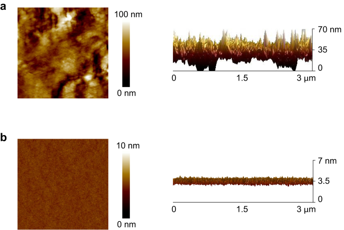
We fabricated GFETs on a Scotch tape made of polytetrafluoroethylene (PTFE, 50 μm). First, the Scotch tape substrate was attached on a SiO2 wafer for ease of fabrication. The as-purchased Scotch tape had a large surface roughness, so a thin polyimide layer (9 μm) was spin-coated on the tape; the polyimide layer significantly reduced the roughness of Scotch tape, as shown in Fig. 3. To create gate electrodes, aluminum was evaporated using a shadow mask on the sample. Then, the gate dielectric was formed on the aluminum layer by oxidizing the surface by oxygen plasma at 12 mTorr, as described above. Gold source/drain electrodes were evaporated on the AlOX gate dielectric using a shadow mask. Finally, a graphene channel with polymeric protective layers was transferred onto the top by using the water-free transfer of graphene, as described in our previous study22. The sample was exposed to neither solvent nor temperatures of more than 150 °C during fabrication. The device structure is shown in Fig. 1a.
Figure 3. Height profile of Scotch tape surface measured by atomic force microscopy.
The scan size is 3 × 3 μm. (a) As-purchased Scotch tape exhibited considerably high surface roughness. Root-mean-square roughness: 28.1 nm. (b) After spin coating of a thin layer of polyimide (9 μm) on the Scotch tape, the surface roughness was significantly reduced to be similar as silicon wafer. Root-mean-square roughness: 0.225 nm.
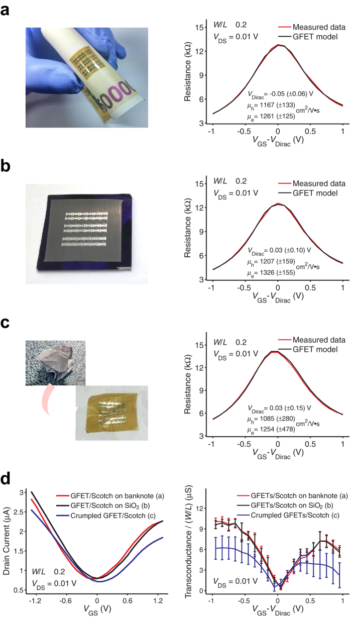
First, we tested the AlOX gate dielectric layer on the Scotch tape substrate. The measured capacitance was 1.5 (±0.3) μF cm−2, which is almost the same as that of the AlOX layer made on a SiO2 substrate. The leakage current through the gate dielectric was an order of magnitude higher, and the breakdown voltage was approximately 0.5 V lower as compared to AlOX on SiO2 (see Supplementary Information Fig. S1). These degraded insulating properties can be attributed to the soft substrate surface, which results in a rough bottom aluminum layer. Nonetheless, the AlOX gate dielectric prepared on Scotch tape exhibited sufficient electrical performance such that it can be used in low-voltage GFETs with a negligible gate leakage. After fabricating the GFETs on the Scotch tape substrate (GFETs/Scotch), the GFETs/Scotch were separated from SiO2 and attached on a banknote by using the adhesive remaining on the backside of Scotch tape (Fig. 4a). The electrical performance of the samples was measured, and the field-effect mobility (μh for holes; μe for electrons) values were extracted from a diffusive transport model of GFET (see Supplementary Information Table S1 for detailed parameters)29. As summarized in Fig. 4a,b, the electrical performance of the GFETs/Scotch did not appreciably change after being transferred onto a banknote. Another set of samples was separated from the SiO2 wafer and attached on office paper. The paper was crumpled and flattened, and the electrical performance of the GFETs/Scotch was measured. As shown in Fig. 4c, GFETs/Scotch still exhibited satisfactory operation after extreme bending and showed only a slight decrease in mobility. In a previous study, a significantly thin layer of plastic foil substrate (2 μm) was used to make crumpled organic transistor arrays30. The notable bending property was attributed to the remarkably low foil thickness, which can sometimes cause difficulties in handling it appropriately. However, the GFETs/Scotch prepared in the present work exhibited sufficient rigidity for facile use and attachment on various objects. The electrical performance of GFETs/Scotch under three different substrate conditions is summarized in Fig. 4d (see Supplementary Information Fig. S2 for drain current vs. drain-to-source voltage curves).
Figure 4. Electrical measurement data of graphene field-effect transistors on Scotch tape (GFETs/Scotch).
The channel width was fixed to 85 μm, and the width-to-length ratio (W/L) values were 0.2 and 0.45. (a–c) Transistor channel resistance vs. gate-to-source voltage curves for GFETs/Scotch attached on different substrates. (a) GFETs/Scotch samples were attached on a banknote. While the samples were bent with a bending radius of 0.5 cm, the electrical properties remained the same (the maximum surface strain was less than 1%, see Fig. 5). (b) As-fabricated GFETs/Scotch on a SiO2 wafer. (c) The GFETs/Scotch on a paper were crumpled, flattened, and measurements were performed. (d) Performance summary of the GFETs/Scotch on the three different substrates. All measurements were performed in ambient air, and more than 10 devices were measured for each sample set.
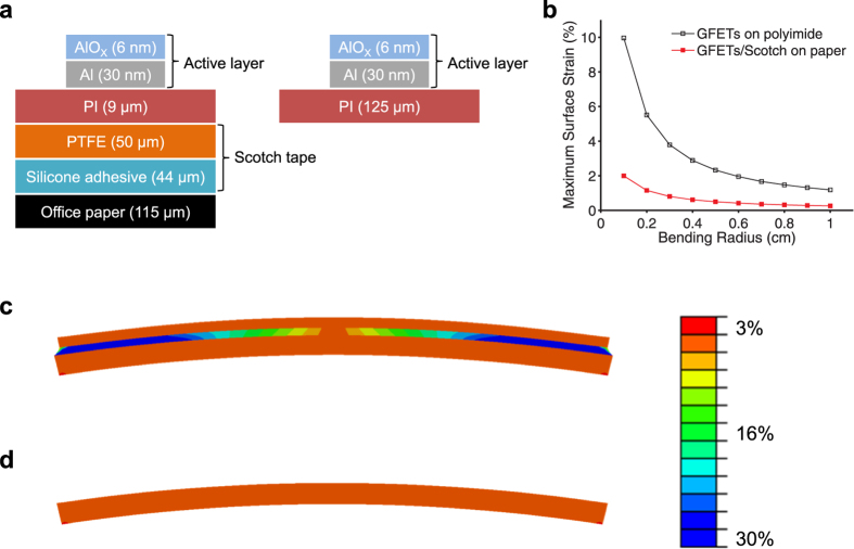
Excessive surface strain induces the formation of cracks or irreversible deformation when a flexible device is bent beyond its limit, which in turn results in permanent device failure. Therefore, the range of feasible bending radii is determined by the maximum surface strain exerted on the active layer. The maximum strain at the top layer of the bent GFETs/Scotch was obtained by employing a finite element analysis with two-dimensional (2D) plain strain condition31. As shown in Fig. 5a, two model structures were studied: Scotch tape attached on a sheet of office paper (Fig. 4c) and a commonly used polyimide film as a control sample. When an oxidized AlOX/Al sample on polyimide was folded, the insulating property of AlOX was completely lost, and crease marks remained. We imposed displacements on the bottom of the structures corresponding to bending radii and measured the lateral strain at the center of the top layer. In Fig. 5b, the Scotch tape sample exhibits a significantly lower surface strain compared to regular polyimide sample by a factor of five at a given bending radius. This numerical analysis can be understood in light of a 2D shear-lag model, which describes strain propagation in multilayers32. When the bottom layer is subject to a uniform strain εbottom, the shear-lag model predicts the maximum strain at the top by Equation 2
Figure 5. Finite element analysis on graphene transistors on Scotch tape.
(a) Model structure for surface stain calculation [left: GFETs/Scotch on office paper; right: GFETs on a polyimide (PI) film]. (b) Surface strain data as a function of bending radius. Although the thickness of the GFETs/Scotch on the office paper is approximately twice that of the GFETs on polyimide, the surface strain on the GFETs/Scotch is five times lower. This result is attributed to the soft silicon adhesive interlayer, which relaxes the strain applied to the top surface. (c,d) Assuming the model structure in (a) is bent with a bending radius of 0.5 cm, the distribution of shear strain is calculated by using a finite element analysis. (c) GFETs/Scotch on office paper. The shear strain is concentrated in the silicone adhesive interlayer where the shear modulus is the lowest. (d) GFETs on a polyimide film. The shear strain is uniformly distributed.
 |
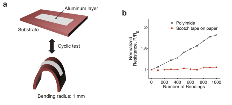
where Ltop is the lateral dimension of the top layer, and Λ is a parameter proportional to the  of the middle layer. The reduced strain in the Scotch tape sample is attributed to its soft silicone adhesive interlayer with a relatively low shear modulus, where mechanical load is not effectively transferred (see Fig. 5c,d). Therefore, the GFETs/Scotch on the office paper can be crumpled with a high degree of bending even though the total film thickness is greater than that of a typical polyimide sample. The effects of the strain-releasing adhesive layer are further corroborated by consecutive bending tests as shown in Fig. 6. A thin layer of aluminum deposited on the two substrate samples (Scotch tape attached on office paper and polyimide film) was bent and released consecutively with a bending radius of 1 mm. In Fig. 6, the aluminum layer on the Scotch tape substrate shows much less resistance increase against the mechanical strain from the bending and releasing, compared with the polyimide substrate. The less change on the resistance of the Scotch tape sample is attributed to its adhesive layer, which reduces the mechanical strain on the top.
Figure 6. Resistance change of metal thin film against consecutive mechanical strain.
(a) Schematic of device structure and experiment. A thin layer of aluminum (thickness: 300 nm; length: 2 cm; width: 0.2 cm) was deposited on a Scotch tape attached on office paper and a polyimide film. Detailed substrate structure is shown in Fig. 5(a). (b) Normalized resistance data of the aluminum layer as a function of the number of bendings. Electrical measurements were performed while the sample was flat. As explained in Fig. 5, the adhesive layer of the Scotch tape relaxes the strain applied to the top; therefore, the aluminum layer on Scotch tape exhibits much less increase on its resistance value against mechanical strain than the aluminum on the regular polyimide substrate.
We demonstrated flexible GFETs on a Scotch tape substrate. The GFETs/Scotch was easily laminated onto diverse nonconventional substrates, such as a pen, human skin, and a banknote, using Scotch tape adhesive. The soft nature of Scotch tape allows for the sample to be crumpled without leading to device failure. From mechanical calculations, we found that the Scotch tape adhesive with a low Young’s modulus relaxes the strain applied to the top surface when the GFETs/Scotch sample is bent. For practical low-power electronic applications, high-quality AlOX was fabricated as the gate dielectric of the GFETs by oxygen plasma treatment. The AlOX exhibited a negligible gate leakage current, and a supply voltage of only 2.5 V was sufficient to operate the GFETs because of its high capacitance of 1.5 μF cm−2. We envision that such a device concept for flexible graphene transistors on Scotch tape can be exploited and extended to ubiquitous electronic applications wherein electronics can be easily placed in any desired position.
Methods
Fabrication of graphene transistors on Scotch tape
Scotch tape (3MTM, 5480) was attached on a silicon dioxide wafer piece. A polyimide solution (VTECTM, PI-1388) was coated onto the Scotch tape sample at 3000 rpm for 30 s, followed by sequential baking at 60 and 150 °C for 10 min. An aluminum layer (30 nm) as gate electrodes was deposited in a thermal evaporator with a shadow mask. The aluminum surface was oxidized in an oxygen plasma chamber with an RF power of 250 W for 7 min to form the gate dielectric layer. During plasma treatment, the oxygen pressure was set to the lowest possible value while maintaining the plasma; the lowest pressure value was 12 mTorr in our plasma chamber. Source/drain electrodes (40-nm-thick gold on 5-nm-thick titanium) were deposited in a thermal evaporator using a shadow mask. Finally, a graphene channel with polymeric protective bilayers was laminated on the top of the sample by employing the water-free transfer method as described in our previous study22. Poly(methyl methacrylate) and polybutadiene were used for supporting bilayers of graphene transfer and for passivation against detrimental ambient species to prevent Fermi level change33,34,35 and charge-impurity scattering36.
Additional Information
How to cite this article: Chung, Y. et al. Ubiquitous Graphene Electronics on Scotch Tape. Sci. Rep. 5, 12575; doi: 10.1038/srep12575 (2015).
Supplementary Material
Acknowledgments
This work was supported by the Center for Advanced Soft Electronics under the Global Frontier Research Program (2012M3A6A5055728) of the Ministry of Science, ICT and Future Planning and by the Basic Science Research Program (NRF-2013R1A1A2012046) through the National Research Foundation of Korea funded by the Ministry of Education. The authors thank Professor Bong Koo Kang for discussions.
Footnotes
Author Contributions Y.C. and H.H.K. conceived the idea and performed experiments and measurements. S.L. and S.R. conducted mechanical simulations. E.L. and S.W.K. performed experiments on strained aluminum films. K.C. directed the research project. Y.C. wrote the paper. All authors discussed the results and commented on the manuscript.
References
- Wong W. S. & Salleo A. Flexible electronics: materials and applications. (Springer, 2009). [Google Scholar]
- Gelinck G. H. et al. Flexible active-matrix displays and shift registers based on solution-processed organic transistors. Nat Mater 3, 106–110 (2004). [DOI] [PubMed] [Google Scholar]
- Someya T. et al. A large-area, flexible pressure sensor matrix with organic field-effect transistors for artificial skin applications. P Natl Acad Sci USA 101, 9966–9970 (2004). [DOI] [PMC free article] [PubMed] [Google Scholar]
- Liu X. T. et al. Flexible, Low-Voltage and High-Performance Polymer Thin-Film Transistors and Their Application in Photo/Thermal Detectors. Adv Mater 26, 3631–3636 (2014). [DOI] [PubMed] [Google Scholar]
- Sun Q. et al. Transparent, Low-Power Pressure Sensor Matrix Based on Coplanar-Gate Graphene Transistors. Adv Mater 26, 4735–4740 (2014). [DOI] [PubMed] [Google Scholar]
- Sekitani T. et al. Organic Nonvolatile Memory Transistors for Flexible Sensor Arrays. Science 326, 1516–1519 (2009). [DOI] [PubMed] [Google Scholar]
- Kim M. et al. Lateral Organic Solar Cells with Self-Assembled Semiconductor Nanowires. Adv Energy Mater 5, 1401317, (2015). [Google Scholar]
- Chen Z. et al. A Three-Dimensionally Interconnected Carbon Nanotube-Conducting Polymer Hydrogel Network for High-Performance Flexible Battery Electrodes. Adv Energy Mater 4, 1400207 (2014). [Google Scholar]
- Ziemelis K. Putting it on plastic. Nature 393, 619–620 (1998). [Google Scholar]
- Kim D. H. et al. Epidermal Electronics. Science 333, 838–843 (2011). [DOI] [PubMed] [Google Scholar]
- Andersson P. et al. Active matrix displays based on all-organic electrochemical smart pixels printed on paper. Adv Mater 14, 1460–1464 (2002). [Google Scholar]
- Zschieschang U. et al. Organic Electronics on Banknotes. Adv Mater 23, 654 (2011). [DOI] [PubMed] [Google Scholar]
- Khan M. A., Bhansali U. S. & Alshareef H. N. High-Performance Non-Volatile Organic Ferroelectric Memory on Banknotes. Adv Mater 24, 2165–2170 (2012). [DOI] [PubMed] [Google Scholar]
- Avouris P. Graphene: Electronic and Photonic Properties and Devices. Nano Lett 10, 4285–4294 (2010). [DOI] [PubMed] [Google Scholar]
- Bae S. et al. Roll-to-roll production of 30-inch graphene films for transparent electrodes. Nat Nanotechnol 5, 574–578 (2010). [DOI] [PubMed] [Google Scholar]
- Wang H., Nezich D., Kong J. & Palacios T. Graphene Frequency Multipliers. IEEE Electron Device Letters 30, 547–549 (2009). [Google Scholar]
- Lee E., Lee K., Liu C. H., Kulkarni G. S. & Zhong Z. H. Flexible and transparent all-graphene circuits for quaternary digital modulations. Nat Commun 3:1018, 10.1038/ncomms2021 (2012). [DOI] [PubMed] [Google Scholar]
- Schwierz F. Graphene transistors. Nat Nanotechnol 5, 487–496 (2010). [DOI] [PubMed] [Google Scholar]
- Chen C. Y. et al. Graphene mechanical oscillators with tunable frequency. Nat Nanotechnol 8, 923–927 (2013). [DOI] [PubMed] [Google Scholar]
- DuPont Fluoroproducts, Teflon® PTFE fluoropolymer resin: Properties Handbook. (DuPontTM Technical Report H-37051-3, 1996); DuPontTM Kapton® HN Technical Data Sheet. (2011) Available at: http://www.dupont.com/content/dam/assets/products-and-services/membranes-films/assets/DEC-Kapton-HN-datasheet.pdf (Accessed: 7th October 2014).
- Lee J. et al. 25 GHz Embedded-Gate Graphene Transistors with High-K Dielectrics on Extremely Flexible Plastic Sheets. ACS Nano 7, 7744–7750 (2013). [DOI] [PubMed] [Google Scholar]
- Kim H. H., Chung Y., Lee E., Lee S. K. & Cho K. Water-Free Transfer Method for CVD-Grown Graphene and Its Application to Flexible Air-Stable Graphene Transistors. Adv Mater 26, 3213–3217 (2014). [DOI] [PubMed] [Google Scholar]
- Kim B. J. et al. High-Performance Flexible Graphene Field Effect Transistors with Ion Gel Gate Dielectrics. Nano Lett 10, 3464–3466 (2010). [DOI] [PubMed] [Google Scholar]
- Thiemann S. et al. Cellulose-Based Ionogels for Paper Electronics. Adv Funct Mater 24, 625–634 (2014). [Google Scholar]
- Klauk H., Zschieschang U., Pflaum J. & Halik M. Ultralow-power organic complementary circuits. Nature 445, 745–748 (2007). [DOI] [PubMed] [Google Scholar]
- Lieberman M. A. & Lichtenberg A. J. Principles of plasma discharges and materials processing. 2nd edn (Wiley-Interscience, 2005). [Google Scholar]
- Chung Y., Murmann B., Selvarasah S., Dokmeci M. R. & Bao Z. N. Low-voltage and short-channel pentacene field-effect transistors with top-contact geometry using parylene-C shadow masks. Appl Phys Lett 96, 133306 (2010). [Google Scholar]
- Powell C. J. & Jablonski A. Evaluation of calculated and measured electron inelastic mean free paths near solid surfaces. J Phys Chem Ref Data 28, 19–62 (1999). [Google Scholar]
- Kim S. et al. Realization of a high mobility dual-gated graphene field-effect transistor with Al2O3 dielectric. Appl Phys Lett 94, 062107 (2009). [Google Scholar]
- Kaltenbrunner M. et al. An ultra-lightweight design for imperceptible plastic electronics. Nature 499, 458 (2013). [DOI] [PubMed] [Google Scholar]
- Bathe K.-J. r. Finite element procedures. (Prentice Hall, 1996). [Google Scholar]
- Sun J. Y. et al. Inorganic islands on a highly stretchable polyimide substrate. J Mater Res 24, 3338–3342 (2009). [Google Scholar]
- Kim H. H. et al. Substrate-Induced Solvent Intercalation for Stable Graphene Doping. ACS Nano 7, 1155–1162 (2013). [DOI] [PubMed] [Google Scholar]
- Kim H. et al. Doping Graphene with an Atomically Thin Two Dimensional Molecular Layer. Adv Mater 26, 8141 (2014). [DOI] [PubMed] [Google Scholar]
- Lee S. K. et al. Inverse Transfer Method Using Polymers with Various Functional Groups for Controllable Graphene Doping. ACS Nano 8, 7968–7975 (2014). [DOI] [PubMed] [Google Scholar]
- Lee W. H. et al. Control of Graphene Field-Effect Transistors by Interfacial Hydrophobic Self-Assembled Monolayers. Adv Mater 23, 3460 (2011). [DOI] [PubMed] [Google Scholar]
Associated Data
This section collects any data citations, data availability statements, or supplementary materials included in this article.


