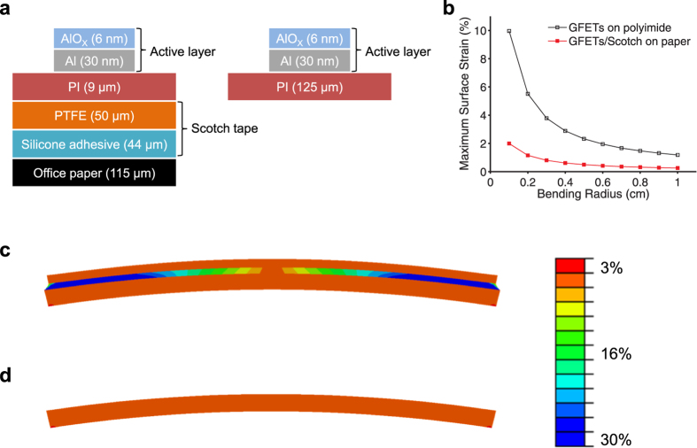
Figure 5. Finite element analysis on graphene transistors on Scotch tape.
(a) Model structure for surface stain calculation [left: GFETs/Scotch on office paper; right: GFETs on a polyimide (PI) film]. (b) Surface strain data as a function of bending radius. Although the thickness of the GFETs/Scotch on the office paper is approximately twice that of the GFETs on polyimide, the surface strain on the GFETs/Scotch is five times lower. This result is attributed to the soft silicon adhesive interlayer, which relaxes the strain applied to the top surface. (c,d) Assuming the model structure in (a) is bent with a bending radius of 0.5 cm, the distribution of shear strain is calculated by using a finite element analysis. (c) GFETs/Scotch on office paper. The shear strain is concentrated in the silicone adhesive interlayer where the shear modulus is the lowest. (d) GFETs on a polyimide film. The shear strain is uniformly distributed.

