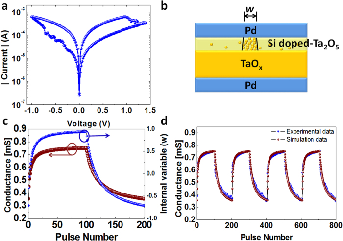
Figure 1.
Memristor device and modeling. (a) DC I-V characteristics of a typical memristor device showing the bipolar switching effect. (b) Schematic of a memristor device. The region with high oxygen vacancy concentration (bounded by the black lines) forms the conduction channel. (c) Calculated memristor conductance and the internal state variable w during the application of 100 potentiation pulses (−1 V, 10 μs) and 100 depression pulses (1.15 V, 10 μs). (d) Measured (blue) and calculated (purple) conductance values measured by a read (0.2 V) pulse during 4 periods of 100 potentiation and 100 depression pulses.

