Abstract
Tungsten doped titanium dioxide films with both transparent conducting oxide (TCO) and photocatalytic properties were produced via aerosol-assisted chemical vapor deposition of titanium ethoxide and dopant concentrations of tungsten ethoxide at 500 °C from a toluene solution. The films were anatase TiO2, with good n-type electrical conductivities as determined via Hall effect measurements. The film doped with 2.25 at.% W showed the lowest resistivity at 0.034 Ω.cm and respectable charge carrier mobility (14.9 cm3/V.s) and concentration (×1019 cm−3). XPS indicated the presence of both W6+ and W4+ in the TiO2 matrix, with the substitutional doping of W4+ inducing an expansion of the anatase unit cell as determined by XRD. The films also showed good photocatalytic activity under UV-light illumination, with degradation of resazurin redox dye at a higher rate than with undoped TiO2.
Transparent conducting oxide (TCO) films have important applications in many opto-electronic devices such as solar cells and display technologies1,2,3,4. They combine electrical conductivity with optical transparency (>80% in the visible region)1,5. Traditional TCO materials are based around Sn doped In2O3 (ITO), however due to the high costs associated with indium, research has been focused on finding alternative materials with comparable conductivity and transparency to ITO4.
Titanium dioxide is a widely used intrinsically n-type semiconductor with primary applications in photocatalysis6,7. Recently, the use of TiO2 as a TCO material has gained widespread attention due to advantageous electronic properties and conductivity arising from d electrons unlike ITO where conductivity is due to s electrons8,9,10.
Furubayashi et al. has shown the possibility of achieving TiO2 thin films with respectable conductivities and transparencies using Nb and Ta as dopants using PLD11,12. Parkin et al. were able to produce Nb and Ta doped TiO2 films via CVD methods with sheet resistances of 6.5 Ω sq−1 and 14 Ω sq−1 respectively as well as resistivites of 1.1 × 10⁻³ Ω.cm and 2.7 × 10⁻³ Ω.cm9,13.
Using W as a dopant is another possibility as it enables the release of up to two electrons for every one dopant atom10,14. This is advantageous as it allows the use of low dopant levels that reduce defect concentrations and hence reduce scattering of charge carriers. W is an ideal dopant that is soluble in a TiO2 matrix because it commonly occurs in the 6+ oxidation state and in that state has a smaller ionic radius than Ti4+.10,14 Hence, there is potential to obtain better conductivity and transparency compared to Nb and Ta. Xu and Chen et al. were able to obtain resistivities in the order of 10−2 Ω.cm via magnetron co-sputtering10.
Furthermore, W doping of TiO2 has multiple advantages, as it is known to enhance the photocatalytic activity by reducing charge carrier recombination and by increasing light absorption by absorbing in the visible portion of the spectrum15.
In this paper we present the first synthesis of W doped TiO2 films via a specialized solution based chemical vapor technique (CVD) known as aerosol assisted (AA) CVD9,16,17,18. It is a simple, versatile and easily scalable technique that involves the transportation of the precursors into the deposition chamber in the form of aerosol droplets19. The films were deposited using a toluene solution of [Ti(OEt)4] and [W(OEt)6] on glass susbstrates at 500 °C and the films were transparent, photocatalyticically active, coloured and conducting - enabling four functional properties in the same film.
Results and Discussion
Thin films of undoped and W doped TiO2 were deposited on glass substrates via AACVD at 500 °C using nitrogen as the carrier gas. An undoped TiO2 film was made from a toluene (25 mL) solution of [Ti(OEt)4], while for the W doped TiO2 films dopant concentrations (2–20 mol.% in solution) of [W(OEt)6] were used. This is to our knowledge the first example of W doped TiO2 being formed by AACVD. All films were well adhered to the substrate passing the ScotchTM tape test. The undoped films were optically transparent and colourless where as the doped films were translucent blue, with the colour intensity increasing with increasing dopant concentration. The films were air stable, showing no change in colour or conductivity after 3 months.
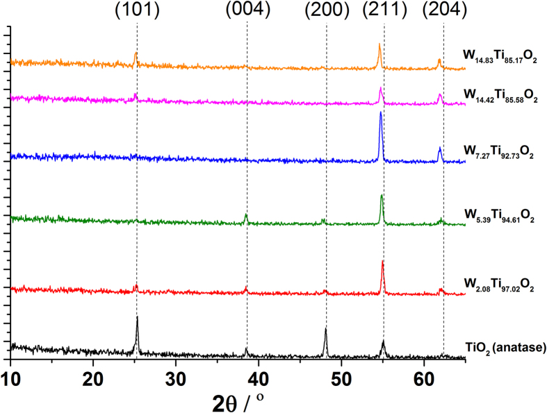
The XRD patterns for the undoped and W doped films show reflections matching the anatase phase of TiO2 (Fig. 1). The undoped film showed peaks corresponding to (101), (004), (200), (211) and (204) planes at 25.3°, 38.7°, 48.2°, 55.1° and 62.4° 2θ respectively. The doped samples showed a degree of preferred orientation in the (211) and (204) directions. This has been previously observed for metal (Nb and Ta) doped TiO2 films deposited using both AACVD and PVD9,13.
Figure 1. The XRD pattern for the undoped and W doped TiO2 films grown via AACVD from a toluene solution of Ti(OEt)4 and W(OEt)6 at 500 °C.
The shift in the peaks to lower 2θ values upon doping with W is indicative of W4+ incorporation into the TiO2 host.
Due to the similarities in the ionic radii of W6+ (0.60 Å) and Ti4+ (0.605 Å), the substitutional doping of W6+ with Ti4+ should impart almost no change in the TiO2 unit cell. However, XPS results (see below) show that doped films contain W in both the 4+ and 6+ oxidation state. Therefore the observed linear shift of the XRD peaks to lower 2θ values, thus indicating an expansion in the TiO2 unit cell, was due to the partial replacement of Ti with W4+ that has an ionic radius of 0.66 Å. This follows closely with observations made by Kafizas and Parkin for W doped TiO2 system studied via combinatorial atmospheric pressure CVD where the majority of the W was in the 5+ oxidation state (0.62 Å)15. The lattice parameters for the undoped and doped films were calculated by fitting a La Bail model to the XRD data using GSAS and EXPGUI programs (Table 1).
Table 1. The table shows the W concentration in the films as determined by WDX as well as the lattice parameter calculations for the undoped and W doped TiO2 films grown via AACVD at 500 °C.
| W content in soln/ mol.% | W:Ti ratio in film / at.% | a / Å | c / Å | Unit cell Vol. / Å3 | Vol. Expansion / % |
|---|---|---|---|---|---|
| 0 | — | 3.7762(1) | 9.431(1) | 134.50(1) | 0 |
| 2 | 0.63 : 29.59 | 3.785985(5) | 9.464915(5) | 135.67(2) | 0.87 |
| 5 | 1.65 : 28.99 | 3.78213(9) | 9.500(2) | 135.89(3) | 1.04 |
| 10 | 2.25 : 28.71 | 3.78287(6) | 9.499(3) | 135.93(4) | 1.07 |
| 15 | 4.47 : 26.52 | 3.7811(8) | 9.51(2) | 136.03(2) | 1.14 |
| 20 | 4.65 : 26.70 | 3.8009(5) | 9.458(2) | 136.64(3) | 1.59 |
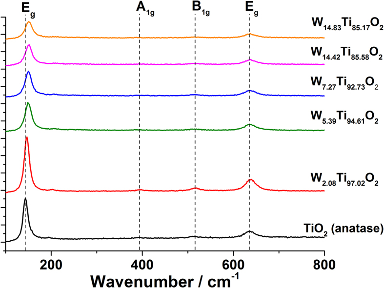
Raman patterns taken for the undoped and W doped TiO2 films showed peaks expected for TiO2 anatase with tetragonal symmetry (Fig. 2)20. Upon doping of TiO2 the main peak (Eg vibrational mode) was shifted to higher wavenumbers indicating an expansion of the unit cell. The shift in the Eg peak increased linearly with increasing W concentration and is consistent with formation of a solid solution as observed by the XRD data.
Figure 2. The Raman spectra for the undoped TiO2 and W doped TiO2 films grown via AACVD.
A linear blue shift in the Eg peak (from 143–158 cm−1) that was observed is indicative of an expansion in the anatase unit cell.
Wavelength dispersive X-ray spectroscopy was used to determine the amount of W present in the films. The results show a linear increase in W content before possible saturation is reached at 15 mol.% of W in the AACVD precursor solution and 4.5 at.% in the films (Table 1).
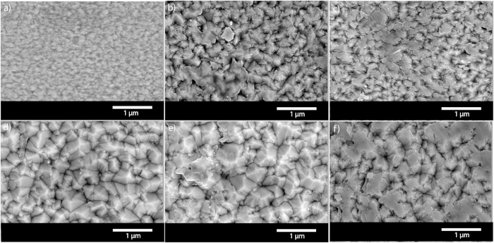
Analysis of the film morphology using scanning electron microscopy (SEM) reveal that the surface of the AACVD grown films become more structured upon doping with W (Fig. 3). The morphology of the undoped TiO2 film consists of compact domes roughly 100 nm in width that transform to pyramidal features perpendicular to the substrate upon W incorporation. With increasing dopant concentration the features coalesce to form larger pyramids that are roughly 500 nm in width. Furthermore, the 4.47 W at.% and 4.65 W at.% films seem to show the features coalescing even further. This has been observed previously when other transition metals such as Nb and Ta have been substituted into a TiO2 matrix9,13. Film thickness, obtained via side-on SEM, show that in general there is an increase in the thickness with increasing amount of dopant. This coupled with the increase in film roughness contributes to a decrease in film transparency.
Figure 3. SEM micrographs of the AACVD grown W doped TiO2 films.
The undoped film (a) shows typical morphology consisting of compact domes. Where as the doped films – 0.63 at.% (b), 1.65 at.% (c), 2.25 at.% (d), 4.47 at.% (e) and 4.65 at.% (f) W concentration - have a more structured morphology consisting of pyramidal features protruding perpendicular to the substrate.
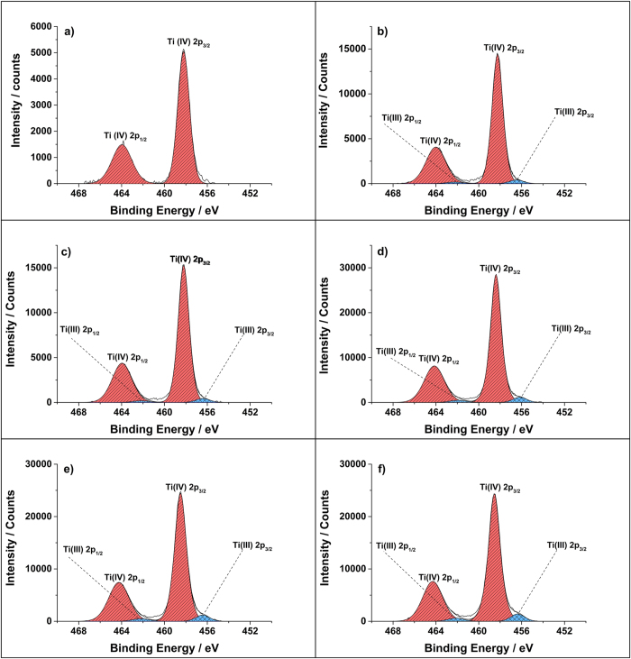
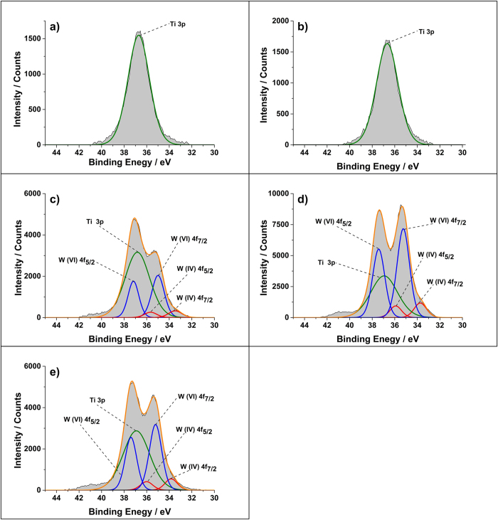
X-ray photoelectron spectroscopy (XPS) was performed on the films to determine the oxidation state of the Ti and W species (Fig. 4 and Fig. 5). For the undoped film a 2p3/2 peak corresponding to Ti in the 4+ oxidation state was observed at 458.3 eV that matches to literature values21,22. The W doped TiO2 samples also showed this peak at 458.2 eV for Ti4+, but an additional 2p3/2 peak at 457.0 eV corresponding to Ti3+ was also observed9,13,23. The intensity of the Ti3+ peak increased with increasing W concentration. Thus indicating that the charge compensation by electrons for the substitutional doping of W 4+ and/or 6+ species for Ti4+ results in the reduction of the titanium to the 3+ oxidation state.
Figure 4. The XPS data for the undoped.
(a) and W doped TiO2 (b-f) films grown via AACVD at 500 °C. There is an increase in the Ti3+ peak intensity with increasing W concentration.
Figure 5. The Ti 2p and W 4f XPS peaks for the W doped TiO2 grown via AACVD.
The intensity of the W 4f peak that coincides at the same region as Ti 2p increases with increasing dopant concentration. Both W 6+ and 4+ is observed.
Peaks corresponding to W 4f overlap with Ti 3s peaks in XPS, therefore W was only detectable for the 2.25 at.% and above doped films (Fig. 5). In these films, 4f7/2 peaks corresponding to W6+ was seen at 35.2 eV as well as 4f7/2 peaks for W4+ at 33.8 eV24,25. There was consistently six times greater W6+ compared to W4+ in all the films. In a previous study where Kafizas and Parkin studied W doping of TiO2 via a combinatorial APCVD method, XPS studies showed the presence of mainly W5+ and some W4+, lacking the desired 6+ oxidation that enables enhanced electrical properties15.
The electrical properties of the doped films were determined though Hall effect measurements with all films displaying n-type conductivity (Table 2). The undoped sample was too resistive to measure on the Hall effect instrument but two-point probe measurements showed conductivity in the MΩ range. With a dopant concentration of 0.63 at.% and 1.65 at.% sheet resistance drops to 4.9 kΩ sq−1 and 3.4 kΩ respectively. For the 0.63 at.% doped sample the resistivity was 0.63 Ω.cm and the charge carrier concentration was to the order of 1017 cm−3 enabling a carrier mobility of 13 cm2/V.s. The resistivity (0.29 Ω.cm), charge carrier concentration (1018 cm3) and mobility (13 cm2/V.s) were also similar for the 1.65 at.% W doped film. A further increase in dopant concentration to 2.25 at.% resulted in the film with the best electrical properties for this study. There was a decrease in sheet resistance and resistivity to 212 Ω.sq−1 and 0.034 Ω.cm respectively. This is comparable to the results obtained by Xu and Jin et al. for W doped TiO2 films grown by rf sputtering. The carrier mobility, at 14.9 cm2/V.s, was slightly better than the 0.63 at.% and 1.65 at.% films while the carrier concentration was an order of magnitude higher. At 4.47 at.% doping of W in TiO2, the sheet resistance was reduced to 78 Ω.sq−1 with a resistivity of 0.042 Ω.cm and an increased carrier concentration in the order of 1020 cm−3. However, the carrier mobility was diminished to 0.32 cm2/V.s (Fig. 3), this is likely to be due to the increased dopant amounts, specifically W in the 4+ oxidation, that behave as scattering sites for the charge carriers. In general, the lower than expected electrical performance of the W doped films synthesisied via AACVD is primarily due to the W4+ center reducing carrier mobility.
Table 2. The electrical properties of the undoped and doped TiO2 films grown via the AACVD reaction of Ti(OEt)4 and W(OEt)6 in toluene at 500 °C as determined by Hall effect measurements.
| W content in soln/mo.l% | W:Ti ratio in film/at.% | Film thickness/μm | Sheet resistance/Ω sq−1 | ρ/Ω.cm | μ/cm2/V.s | N/cm−3 |
|---|---|---|---|---|---|---|
| 0 | — | — | — | — | — | |
| 2 | 0.63 : 29.59 | 1.3 | 4861 | 0.63 | 13.0 | 7.63 × 10¹⁷ |
| 5 | 1.65 : 28.99 | 0.8 | 3433 | 0.29 | 13.4 | 1.64 × 10¹⁸ |
| 10 | 2.25 : 28.71 | 2.8 | 212 | 0.034 | 14.9 | 1.23 × 10¹⁹ |
| 15 | 4.47 : 26.52 | 5.4 | 78 | 0.042 | 0.32 | 4.70 × 10²⁰ |
| 20 | 4.65 : 26.70 | 4.1 | 154 | 0.063 | 0.049 | 2.02 × 10²¹ |
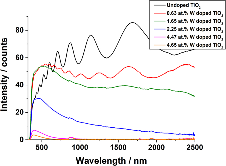
UV-Vis spectroscopy was used to show the optical transmission of the undoped and doped TiO2 films (Fig. 6). The undoped film was transparent in the visible region with 55% transmission, this was similar to the 0.63 at.% doped film that also showed transmission close to 55%. With increasing dopant concentration, the films become less transparent - transmission at a wavelength of 500 nm was roughly 50%, 30%, 7% and 3% for the 1.65 at.%, 2.25 at.%, 4.47 at.% and 4.67 at.%. The decrease in transmission has been observed previously for other transition metal doped TiO2 films and is attributed to the increase in absorption in the infrared region (see supporting information for reflectance and absorption curves)9,13. Furthermore, the transmission of the films decreases from 600 nm most likely due to Ti3+ states induced by the W doping that give rise to absorption from d-d transitions.
Figure 6. The UV-Vis transmission data for the W doped TiO2 films grown from the AACVD reaction of Ti(OEt)4 and W(OEt)6.
The UV light induced photocatalytic properties of the undoped and W doped TiO2 films were determined using resazurin dye based ‘intelligent ink’. The ink contained resazurin dye, hydroxyl-ethyl cellulose, glycerol and distilled water. The degradation of the dye on the surface of the films was induced by a UVA (365 nm) light source with a photon flux of 1.09 × 10¹⁵ photons/cm2/s. The reduction in the concentration of the dye with time was monitored using UV-Vis spectroscopy. The formal quantum efficiency (FQE) and formal quantum yield (FQY) were calculated to enable easy comparison with literature.
The undoped TiO2 film was able to degrade resasurin at a rate of 1.4 × 10¹¹ dye molecules/s/cm2, this was inferior to the 0.63 at.%, 1.65 at.% and 2.25 at.% W doped TiO2 films that had a degradation rate of 3.2 × 10¹¹, 3.5 × 10¹¹ and 2.4 × 10¹¹ dye molecules/s/cm2 respectively. However at 4.47 at.% and 4.65 at.% doping levels the rates of degradation (7.9 × 10¹⁰ dye molecules/s/cm2 for both) was inferior to the undoped TiO2 film. Furthermore, compared to SGG BiocleanTM self-cleaning glass, that was able to degrade resazurin dye at 1.2 × 10¹¹ dye molecules/s/cm2 all the films excluding the 4.47 at.% and 4.65 at.% doped films were superior.
This shows that the presence of W in the TiO2 films does indeed enhance the photocatalytic properties but excess dopants can also be detrimental. The initial increase in the photocatalytic properties of the films with doping was most likely due to the increase in surface microstructure (and also due to the decrease in grain boundaries that are charge carrier recombination sites) due to larger, better shaped particles as observed from the SEM images. This facilitates a high surface area and more photoactive sites for the dye to be degraded during UVA illumination. With excess dopant concentrations (4.47 at% and 4.65 at.%) an increase in the surface area is off set by the presence of more photoinduced charge carrier recombination sites that in total reduce the photoactivity.
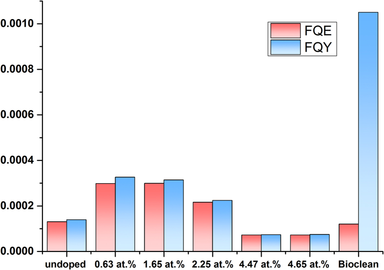
The formal quantum efficiency (FQE) and yield (FQY) for the films were calculated using the dye degradation rates, the UVA photon flux and UVA photon absorption for each of the films (Fig. 7). The 0.63 at.% and 1.65 at.% doped films showed the best results, with a FQE of 2.98 × 10⁻⁴ dye molecules per incident photon and FQY of 3.26 × 10⁻⁴ dye molecules per absorbed photon for the 0.63 at.% doped film and 2.99 × 10⁻⁴ dye molecules per incident photon (FQE) and 3.14 × 10⁻⁴ dye molecules per absorbed photon (FQY) for the 1.65 at.% doped film. This was more than double what was observed for the undoped TiO2 film grown under the same conditions. The principle reason for this was the more structured surface morphology observed for the doped films compared to the undoped. Furthermore, the FQEs of the 0.63 at.% and 1.65 at.% W doped films were also both more than double what was observed (1.2 × 10⁻⁴ dye molecules per incident photon) for SGG BiocleanTM. The FQY of SGG BiocleanTM was however far superior with results an order of magnitude higher than the best preforming W doped TiO2 film.
Figure 7. The graph shows the comparison of the FQE and FQY of the photodegradation of resazurin redox dye on the undoped and doped TiO2 films grown via AACVD.
The FQE and FQY for an industry standard BiocleanTM is also shown.
Compared to literature, the W doped films display the same order of photocatalytic activity (FQE and FQY) relative to W doped TiO2 films studied by combinatorial APCVD15. Resazurin based redox dye test preformed on Pilkington ActivTM self-cleaning glass by Mills et al. shows a FQE of 2.5 × 10⁻⁴ dye molecules/incident photon26. This is in the same order of magnitude as what was observed for the W doped TiO2 samples in this study, indicating the films are on par with industry standards.
Conclusion
Transparent, electrically conductive and photocatalytically active thin films of W doped TiO2 films were synthesisied via a solution based CVD technique (AACVD). The structured morphology of the doped films combined with the good conductivites (optimum of 0.034 Ω.cm) and optical transparency in the visible region make them suitable candidates for electrodes in photovoltaic devices. Furthermore, the doped films displayed enhanced photocatalytic activity compared to the undoped TiO2 sample in the destruction of resazurin redox dye when illuminated by UVA radiation. In conclusion, this paper presents the single step formation of W doped TiO2 films with four desirable functional properties:
Transparent in the visible region
Photocatalytically active
Coloured
Electrically conducting
Methods
General Procedure
Depositions were carried out under nitrogen (99.99% from BOC). Precursors were placed in a glass bubbler and an aerosol mist was created using a piezoelectric device. All chemicals were procured from Aldrich and were utilised as recieved.
[Ti(OEt)4] (2 g, 8.8 mmol) was dissolved in toluene (25 ml) and [W(OEt)5] was added in dopant amounts (0 mol.% – 20 mol.%). The resulting solution was stirred for 30 minutes and then atomised. The precursor flow was kept at 1 L.min−1. The substrate temperature was kept at 500 °C. Deposition time was 45 minutes. After the deposition the bubblers were closed and the substrates were cooled under a flow of nitrogen.
At the end of the deposition the nitrogen flow through the aerosol was diverted and only nitrogen passed over the substrate. The glass substrate was allowed to cool with the graphite block to less than 100 °C before it was removed. Coated substrates were handled and stored in air. The coated glass substrate was cut into ca. 1 cm × 1 cm squares for subsequent analysis.
Film Analysis
Powder X-ray diffraction (PXRD) was used to analyse the samples in a modified Bruker-Axs D8 diffractometer with parallel beam optics equipped with a PSD LynxEye silicon strip detector to collect diffracted X-ray photons. This instrument uses a Cu source for X-ray generation with CuKα1 and CuKα2 radiation of wavelengths 1.54056 Å and 1.54439 Å respectively, emitted with an intensity ratio of 2:1, a voltage of 40 kV and current of 30 mA. The incident beam angle was kept at 1° and the angular range of the patterns collected was 20° < 2θ < 66° with a step size of 0.05° counted at 0.5 s/sep.
Scanning Electron Microscopy (SEM) was performed to determine surface morphology and film thickness using a JEOL JSM-6301F Field Emission SEM at an accelerating voltage of 5 kV.
The W:Ti at.% composition was investigated via wavelength dispersive X-ray (WDX) analysis on a Phillips instrument. The average W:Ti % over four area scans (200 mm2) of each position analysed was taken.
X-ray photoelectron spectroscopy (XPS) was performed using a Thermo Scientific K-alpha photoelectron spectrometer using monochromatic Al-Kα radiation. Survey scans were collected in the range 0–1100 eV (binding energy) at a pass energy of 160 eV. Higher resolution scans were recorded for the principal peaks of Ti (2p), W (4f), O (1s), C (1s) and Si (2p) at a pass energy of 50 eV. Peak positions were calibrated to carbon (284.5 eV) and plotted using the CasaXPS software.
UV/Visible/near IR spectra were taken using a Perkin Elmer Fourier transform Lambda 950 UV/Vis spectrometer over a wavelength range of 300 nm to 2500 nm in transmission mode. The transmission spectra were taken against an air background.
Hall effect measurements were carried out using the van Der Pauw method to determine the sheet resistance, free carrier concentration (N) and mobility (μ). A square array of ohmic contacts arranged on 1 cm2 samples were then subjected to an input current of 1 mA and a calibrated magnetic field of 0.58 T. The transverse voltage was then measured. The measurement was repeated by reversing the direction of the magnetic field and the current.
Prior to the photocatalysis study, the samples were washed with distilled water, rinsed in isopropanol and irradiated for 30 minutes with UVA light to clean and activate the surface. The photocatalysis test involved spray coating the samples with an even layer of the resazurin based ‘intelligent ink’ (with modifications to the original recipe used by Mills et al.). The intelligent ink consisted of resazurin (40 mg) redox dye in an aqueous solution (40 mL) with glycerol (3 g) and hydroxyl-ethyl cellulose (0.45 g). The mixture was aged for 24 hours in a fridge (2–5 °C) and thoroughly mixed before use.
UVA light (flux = 1.01 × 10¹⁵ photons/cm2/s) was used to induce the photoreduction of the resazurin redox dye on the surface of the films and a UV-visible spectrometer was employed to monitor the degradation of the dye. Formal quantum efficiency (FQE) was calculated by dividing the rate of dye molecules destroyed (cm−2 s−1) by the photon flux (1.01 × 10¹⁴ photons cm−2 s−1). The formal quantum yield (FQY) was calculated by dividing the rate of dye molecules destroyed (cm−2 s−1) by the number of photons absorbed (cm−2 s−1) by the film. The photon flux and photon absorption for each film was determined using a UVX radiometer with a detector for 365 nm radiation attached.
Additional Information
How to cite this article: Sathasivam, S. et al. Tungsten Doped TiO2 with Enhanced Photocatalytic and Optoelectrical Properties via Aerosol Assisted Chemical Vapor Deposition. Sci. Rep. 5, 10952; doi: 10.1038/srep10952 (2015).
Supplementary Material
Acknowledgments
Thanks to Dr. Ainara Garcia Gallastegui for useful discussions and Mr. Kevin Reeves for assistance with SEM imaging. Thanks also to Pilkington NSG for the glass substrates. The project was funded by the Deanship of Scientific Research (DSR), King Abdulaziz University, Jeddah under grant no. D-1-434. The authors, therefore, acknowledge DSR with thanks for their technical and financial support.
Footnotes
Author Contributions S.S. and D.S.B. designed/carried out the experiments, preformed the sample characterization measurements and analyzed all the results. S.S. wrote the manuscript. S.S. and Y.L. made the figures for the manuscript. N.C. preformed some of the XPS measurements. C.J.C. and I.P.P. supervised S.S, D.S.B, Y.L. and N.C. and were involved in the design of experiments, editing of the manuscript and discussions through out the work. S.A.A. was involved in a number of scientific discussions and analysis of results. A.O.A. generated ideas and spearheaded the initial collaboration between the institutions. S.N.B. was involved with a number of scientific discussions and analysis of results and has provided valuable insights, which have in turn, directed the research.
References
- Tadatsugu M. Transparent conducting oxide semiconductors for transparent electrodes. Semicond. Sci. Technol. 20, S35 (2005). [Google Scholar]
- Pasquarelli R. M., Ginley D. S. & O’Hayre R. Solution processing of transparent conductors: from flask to film. Chem. Soc. Rev. 40, 5406–5441 (2011). [DOI] [PubMed] [Google Scholar]
- Lewis B. G. & Paine D. C. Applications and processing of transparent conducting oxides. MRS Bull. 25, 22–27 (2000). [Google Scholar]
- Ginley D. S. & Bright C. Transparent conducting oxides. MRS Bull. 25, 15–18 (2000). [Google Scholar]
- Minami T. New n-type transparent conducting oxides. MRS Bull. 25, 38–44 (2000). [Google Scholar]
- Linsebigler A. L., Lu G. & Yates J. T. Jr Photocatalysis on TiO2 surfaces: principles, mechanisms, and selected results. Chem. Rev. 95, 735–758 (1995). [Google Scholar]
- Feng X. et al. Vertically aligned single crystal TiO2 nanowire arrays grown directly on transparent conducting oxide coated glass: synthesis details and applications. Nano Lett. 8, 3781–3786 (2008). [DOI] [PubMed] [Google Scholar]
- King P. D. C. & Veal T. D. Conductivity in transparent oxide semiconductors. J. Phys. Condens. Matter 23, 10.1088/0953-8984/23/33/334214 (2011). [DOI] [PubMed] [Google Scholar]
- Bhachu D. S. et al. Solution Processing Route to Multifunctional Titania Thin Films: Highly Conductive and Photcatalytically Active Nb:TiO2. Adv. Funct. Mater. 24, 5075–5085 (2014). [Google Scholar]
- Chen D.-m. et al. W-doped anatase TiO2 transparent conductive oxide films: Theory and experiment. J. Appl. Phys. 107, dx.doi.org/10.1063/1.3326940 (2010). [Google Scholar]
- Furubayashi Y. et al. A transparent metal: Nb-doped anatase TiO2. Appl. Phys. Lett. 86, 252101–252103 (2005). [Google Scholar]
- Hitosugi T. et al. Ta-doped anatase TiO2 epitaxial film as transparent conducting oxide. Jpn. J. Appl. Phys. 44, L1063 (2005). [Google Scholar]
- Bawaked S. M. et al. Aerosol assisted chemical vapor deposition of conductive and photocatalytically active tantalum doped titanium dioxide films. J. Mater. Chem. A 2, 12849–12856 (2014). [Google Scholar]
- Couselo N., García Einschlag F. S., Candal R. J. & Jobbágy M. Tungsten-Doped TiO2 vs Pure TiO2 Photocatalysts: Effects on Photobleaching Kinetics and Mechanism. J. Phys. Chem. C 112, 1094–1100, 10.1021/jp0769781 (2008). [DOI] [Google Scholar]
- Kafizas A. & Parkin I. P. Combinatorial atmospheric pressure chemical vapor deposition (cAPCVD): a route to functional property optimization. J. Am. Chem. Soc. 133, 20458–20467 (2011). [DOI] [PubMed] [Google Scholar]
- Marchand P., Hassan I. A., Parkin I. P. & Carmalt C. J. Aerosol-assisted delivery of precursors for chemical vapour deposition: expanding the scope of CVD for materials fabrication. Dalton Trans. 42, 9406–9422 (2013). [DOI] [PubMed] [Google Scholar]
- Sathasivam S. et al. Solution Processing of GaAs Thin Films for Photovoltaic Applications. Chem. Mater. 26, 4419–4424 (2014). [Google Scholar]
- Ponja S. et al. Aerosol assisted chemical vapour deposition of hydrophobic TiO2–SnO2 composite film with novel microstructure and enhanced photocatalytic activity. J. Mater. Chem. A 1, 6271–6278 (2013). [Google Scholar]
- Bhachu D. S., Sathasivam S., Carmalt C. J. & Parkin I. P. PbO-Modified TiO2 Thin Films: A Route to Visible Light Photocatalysts. Langmuir 30, 624–630 (2014). [DOI] [PubMed] [Google Scholar]
- Ohsaka T., Izumi F. & Fujiki Y. Raman spectrum of anatase, TiO2. J. Raman Spectrosc. 7, 321–324 (1978). [Google Scholar]
- Erdem B. et al. XPS and FTIR surface characterization of TiO2 particles used in polymer encapsulation. Langmuir 17, 2664–2669 (2001). [Google Scholar]
- Kuznetsov M. V., Zhuravlev J. F. & Gubanov V. A. XPS analysis of adsorption of oxygen molecules on the surface of Ti and TiNx films in vacuum. J. Electron Spectrosc. Relat. Phenom. 58, 169–176, dx.doi.org/10.1016/0368-2048(92)80016-2 (1992). [Google Scholar]
- Chan C. M., Trigwell S. & Duerig T. Oxidation of an NiTi alloy. Surf. Interface Anal. 15, 349–354, 10.1002/sia.740150602 (1990). [DOI] [Google Scholar]
- Biloen P. & Pott G. T. X-ray photoelectron spectroscopy study of supported tungsten oxide. J. Catal. 30, 169–174, dx.doi.org/10.1016/0021-9517(73)90063-8 (1973). [Google Scholar]
- Ng K. T. & Hercules D. M. Studies of nickel-tungsten-alumina catalysts by x-ray photoelectron spectroscopy. J. Phys. Chem. 80, 2094–2102, 10.1021/j100560a009 (1976). [DOI] [Google Scholar]
- Mills A., Wang J. & McGrady M. Method of Rapid Assessment of Photocatalytic Activities of Self-Cleaning Films. The Journal of Physical Chemistry B 110, 18324–18331, 10.1021/jp063577x (2006). [DOI] [PubMed] [Google Scholar]
Associated Data
This section collects any data citations, data availability statements, or supplementary materials included in this article.


