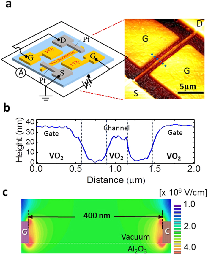
Figure 1. VO2 nanowire device with planer-type gates.

(a) The typical device architecture and an atomic force microscope (AFM) image of the VO2 channel area. S, D and G indicate the source, drain and gate electrodes, respectively. (b) Cross-sectional AFM image, taken at the blue dashed line in (a). (c) Cross-sectional electric field map, determined using finite element analysis at VG = 100 V through the 400-nm vacuum gap between G and the channel (c) on an Al2O3 substrate under vacuum.
