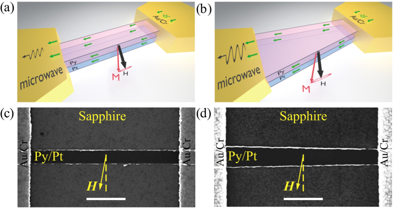
Figure 1. Samples.
Schematic of the straight (a) and tapered (b) nanowire STO: applied magnetic field, electric bias current and precessing magnetization are shown by black, green and red arrows, respectively. Scanning electron micrographs (SEM) of the straight (c) and tapered (d) nanowire STO samples. 500 nm white scale bars are shown in each SEM image.

