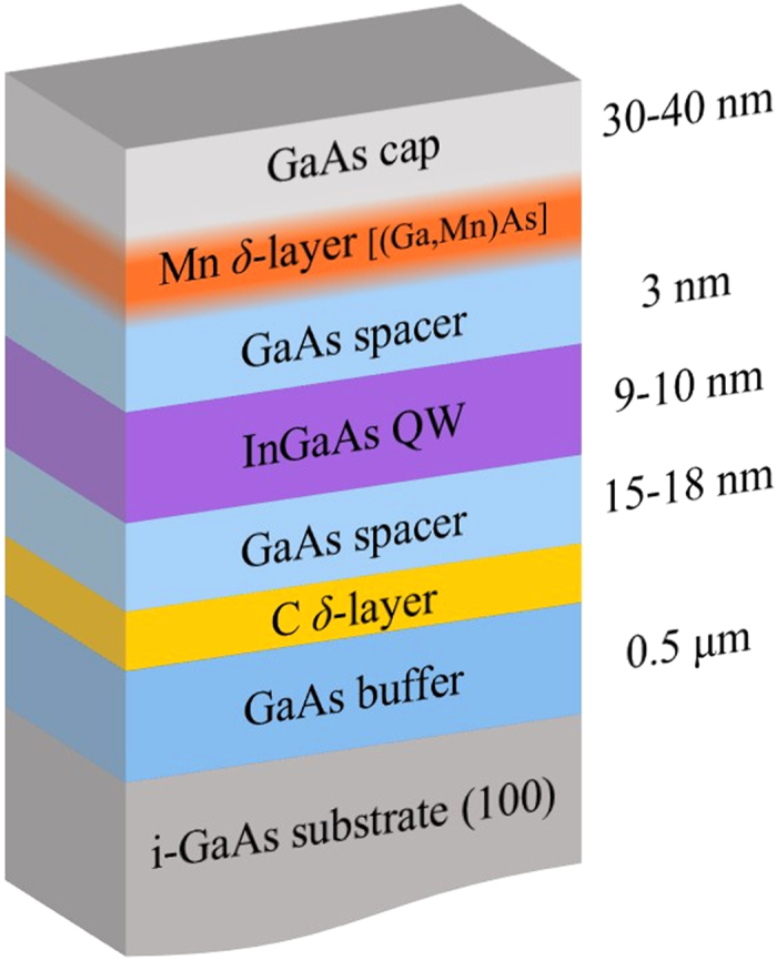
Figure 1. Schematic layout of the two-dimensional magnetic semiconductor heterostructures used in the study.

Resistivity and Hall measurements are performed for the InGaAs quantum well (QW) layer. The Mn δ–doping, which in reality is a (Ga, Mn)As layer (see text) due to diffusion of Mn atoms in the GaAs host, is a source of charge carriers as well as ferromagnetism. The intensity of shading of the Mn layer indicates the inhomogeneity of the doping due to diffusion of Mn atoms. The carbon δ–layer provides additional holes to make the GaAs layer a p-type semiconductor, while the buffer layer is intrinsic GaAs. The heterostructure design provides a favourable platform for gate control of ferromagnetic properties.
