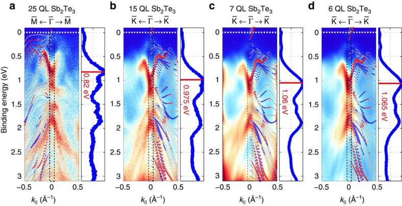
Figure 3. Wide energy EB versus k|| ARPES maps.
25 QL (a) 15 QL (b) 7 QL (c) and 6 QL (d) Sb2Te3 samples measured along indicated crystallographic directions using hν=21.22 eV. The electronic structure of a 6 QL-thick Sb2Te3 slab calculated by DFT along the corresponding crystallographic direction is superimposed. Red and blue dots in this calculation refer to opposite in-plane spin orientation. The Fermi level is indicated by the white dashed line. The energy distribution curves (EDCs) which are integrated over the black dashed area are shown on the right of each ARPES map and mark the energetic position of the most prominent features. The main feature being the bottom of the lower Rashba-split surface state serves as a gauge for the observed energetic shift.

