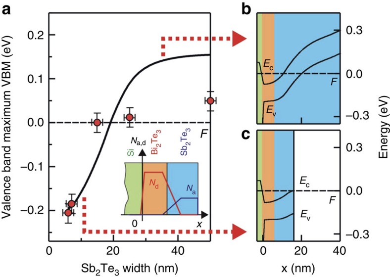
Figure 5. Result of the 1D model using Schrödinger–Poisson equation.
(a) Calculated energetic position of the valence band maximum with respect to the Fermi level at the surface to vacuum for different Sb2Te3 layer thicknesses (black line) and experimentally derived values of the VBM from ARPES (red dots). A large error of ±25 meV was estimated on the position of the VBM because determination from ARPES is difficult. An error of ±2 nm was assumed on the accuracy of the film thickness from combined X-ray reflectivity and transmission electron microscopy investigations. The model assumes the creation of a depletion layer, which causes band bending. (b) and (c) show the band diagram of both valence and conduction band throughout the entire system for top layer thicknesses of 35 nm and 10 nm, respectively (connected by red dashed arrows to the curve in a). Green is the Si substrate, orange is Bi2Te3 and blue is Sb2Te3.

