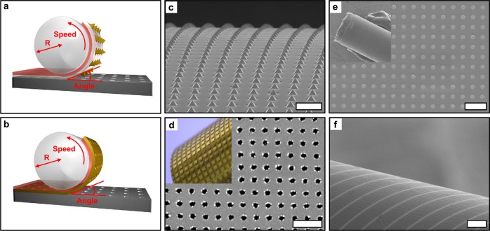
Figure 4.
(a) Illustration of a roller template stripping process. Patterned metals on a silicon template are covered with a PDMS transfer layer (white) followed by a sticky double-sided Kapton tape (red). A glass rod lens is used as a rollable substrate to peel off patterned metals from the Si substrate and wrap them around its cylindrical surface. (b) Gold nanohole array films can be transferred using only a Kapton tape layer. (c) An array of 7 μm sized pyramids was rolled onto the curved surface of a glass rod (2 mm in diameter). Scale bar: 20 μm. (d) Nanohole patterns transferred onto a glass rod with a 10 mm diameter. The nanohole array with a 500 nm period and a 200 nm hole size was separated into 200 μm by 200 μm square patterns via standard photolithography before transferring to the glass rod. Scale bar: 1 μm. (e) An array of Au disks (200 nm diameter) was integrated onto the surface of a 1 mm radius glass rod using an optical epoxy transfer layer. Scale bar: 1 μm. (f) An array of parallel Au wires (5 μm width) was transferred onto a glass rod (2 mm diameter) with optical epoxy and a Kapton tape transfer layer. Scale bar: 30 μm.

