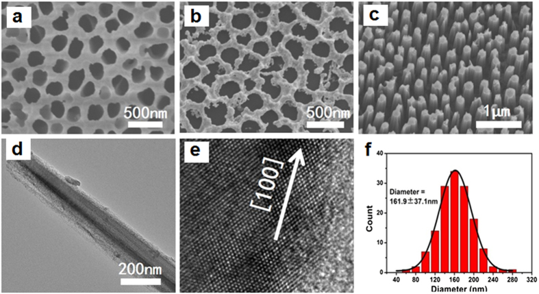
Figure 1.
(a,b) SEM images of a Au-coated AAO membrane and a Au mesh-coated silicon wafer, respectively; (c) SEM image of SiNWs; (d) TEM diagram of an individual SiNW; (e) HRTEM diagram of a SiNW; (f) Histogram of the SiNWs diameter distribution, together with a Gaussian fit (solid line) of the measured statistical data.

