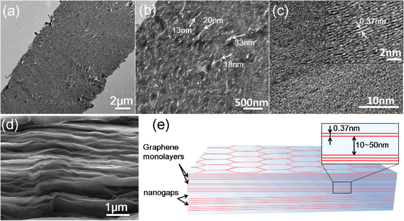
Figure 2. Morphology and structure of graphene film.
(a) Low-, (b) middle-, and (c) high-resolution TEM cross-sectional images of the graphene film, which were obtained under a 300 keV electron beam. The arrows in (b) indicate the nanogaps of ~10–50 nm. The inset in (c) shows an image of the highest resolution. (d) SEM image of the fracture edge of the graphene film. (e) Schematic drawing of the structure of the graphene film.

