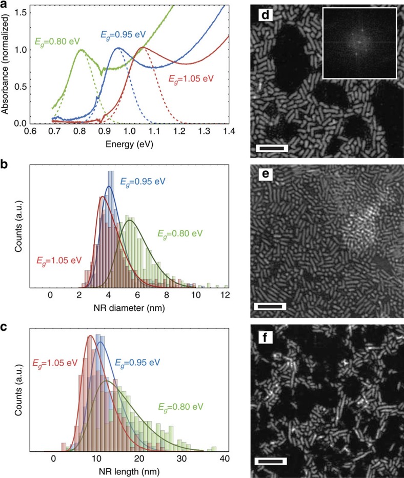
Figure 1. Analysis of synthesized NRs.
(a) Normalized absorbance spectra of three different CdCl2-treated PbSe NR samples in solution. The feature at 0.88 eV is an artefact due to the detector change during the absorbance measurement. (b) Short- and (c) long-axis distribution of the same bandgap PbSe NRs as determined by scanning transmission electron microscopy (TEM). High-angle annular dark-field (HAADF) TEM images for 0.80, 0.95 and 1.05 eV bandgap samples are shown in d–f. To confirm the lattice parameters of PbSe in the synthesized NRs, we extract an FFT image from a high-resolution TEM for the 0.8 eV bandgap sample (see inset in d). Further TEM and XPS analysis and optimatization details are provided in the Supplementary Figs 1, 2 and 3, respectively. Scale bars, 25 nm (d–f).

