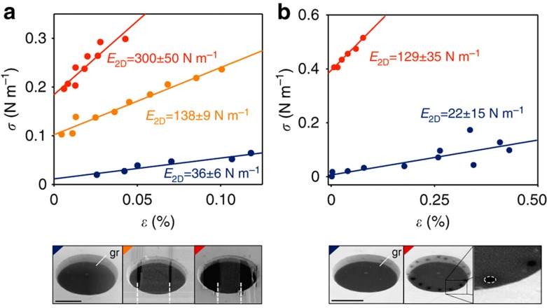
Figure 4. Probing changes of stiffness in devices with varying geometry.
(a) Stress (σ) versus strain (ɛ) curves for a single graphene device as its aspect ratio is changed via FIB lithography. SEM images of the device at each step of cutting are shown in bottom panels (cut directions are white dashed lines). (b) Stress-strain curves for another device as it is perforated near the edge of the membrane. SEM image of the device before and after perforations is shown in bottom panels. Scale bar, 5 μm.

