Figure 2.
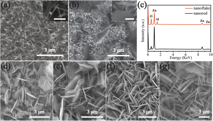
Top view SEM images of (a) AZ1-C (1 mM, without MCU) (b) AZ1 (1 mM with MCU); (c)corresponding EDS of NF and NR in sample AZ1; (d–g) the ZnO/AZO nanostructures obtained with MCU by varying Al reactant supply concentration: (d) AZ2 (2 mM), (e) AZ3 (3 mM), (f) AZ4 (4 mM) and (g) AZ5 (5 mM). The scale bar in inset of (a,b) is 500 nm.

