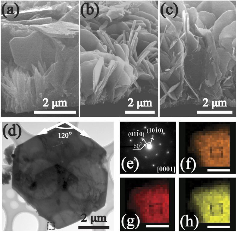
Figure 3.
Side-view SEM images of reprezented AZO nanostructures (a) AZ1, (b) AZ2 and (c) AZ4.(d) TEM images of a single nanoflake from AZ4; (e) The corresponding SAED pattern of AZ4; (f–h) Element mapping of Zn, Al and O in a selected area (high light by dot line cube in (d)) of the nanoflake, scale bar is 100 nm.

