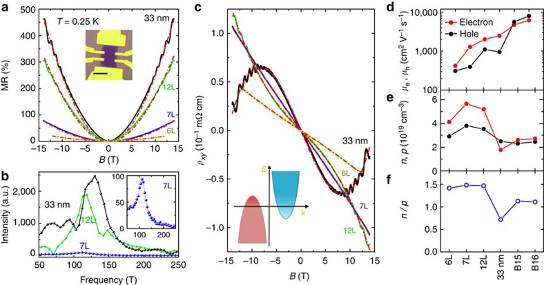
Figure 2. Evolution of magnetotransport in WTe2 crystals from bulk to the atomic scale.
(a) The continuous lines represent the longitudinal MR measured in exfoliated crystals of different thickness (black, 33 nm; green, 12 layers −12L; blue; 7 layers −7L; dark yellow, 6 layers −6L). The red dashed-dotted lines are theoretical fits to equation (3) in the main text. Just as for the bulk, the MR does not saturate, is quadratic throughout the experimental range, and is perfectly reproduced by theory. The inset shows an optical image of a 7L device (scale bar, 5 μm). SdH oscillations superimposed on the measurements of all devices are also visible down to a thickness of 7L, starting from increasingly larger magnetic field values. The corresponding spectra of the oscillations are shown in panel b and its inset; at small thicknesses the smaller number of periods visible in the oscillations decreases the frequency resolution, limiting the visible peak substructure. (c) Transverse resistivity ρxy of the same devices for which the MR is shown in panel a. The different functional dependencies observed for different thicknesses are fully reproduced by equation (2) in the main text (red dashed-dotted lines; all measurements in this figure are done at T=250 mK). The inset shows a schematic representation of the low-energy electronic structure of a two-band semimetal. Panels d–f summarize the evolution of the electron (red) and hole (black) mobility, density and their ratio (density), respectively, as extracted from fitting the data to equations (2) and (3).

