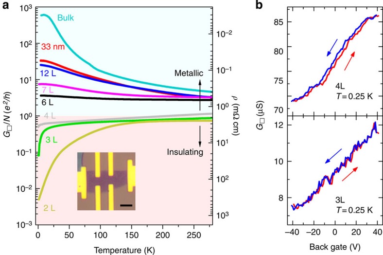
Figure 3. Metal–insulator transition in atomically thin WTe2.
(a) Temperature dependence of the conductance per square normalized to the number of layers, G□/N, measured in crystals of different thickness (from bulk to bilayer −2L) as a function of temperature T (the right axis gives the corresponding resistivity values). The occurrence of a metal–insulator crossover is clearly apparent, with the six-layer (6L) device being still metallic and the four-layer one (4L) being the first for which insulating behaviour is observed. Note how the transition from metallic to insulator occurs at a conductivity per layer that is ∼e2/h. The inset is an optical image of a bilayer device (scale bar, 5 μm). (b) Square conductance, G□, of a trilayer (3L, top) and 4L (bottom) as a function of gate voltage, VG, measured at T=250 mK and B=0 T (the crystals are mounted on a highly doped silicon wafer acting as a gate, covered by a 285 nm SiO2 layer acting as gate insulator). The red and blue curves correspond to data taken on sweeping the gate voltage in opposite directions, as indicated by the arrows of the corresponding colour, and illustrate the reproducibility of the measurements.

