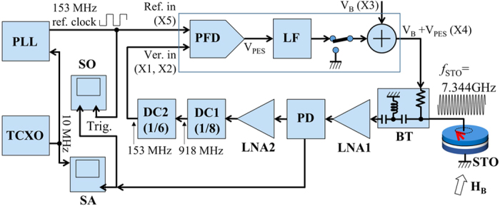
Figure 4. Detailed block diagram of the PLL built in this work.

Each functional block is labeled as follows. STO: Spin torque oscillator, BT: Bias-Tee, LNA1: 1st Low Noise Amplifier, PD: Power Divider, LNA2: 2nd Low Noise Amplifier, DC1: 1st Down Counter (fixed to 8), DC2: 2nd Down Counter (programmed to 6), PFD: Phase Frequency Detector, LF: Loop Filter, SA: Spectrum Analyzer, SO: Sampling Oscilloscope, TCXO: Temperature compensated crystal oscillator generating 10 MHz master clock, PLL: PLL synthesizer generating 153 MHz reference signal. The detailed explanation about the functionality of each block and operation principle are given in Method. The labels X1–X5 are the connector ID shown in the circuit diagram (Figure s1) in Supplementary information.
