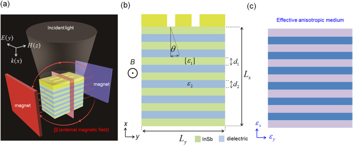
Figure 1. Concept for magnetically controlled subwavlength resolution setup.
(a) A diagram of setup. (b) Side-view of the layered semiconductor-dielectric structure under an external magnetic field B (viewed from the gray cut plane shown in (a)). The center-to-center distance between two resolved slits carved on Cr mask is 100 μm. The width of the both resolved slits is 50 μm. Lx = 130 μm (Ly = 440 μm) is the x-direction (y-direction) length of layered system. d1 = d2 = 10 μm. θ denotes the angle between the propagation direction and the normal direction. (c) Structure equivalent to (b), which includes the effect of external magnetic field.

