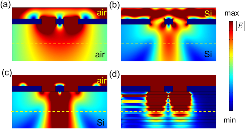
Figure 6. Simulated time-averaged power flow contours for double slits embedded in different materials at incident frequency of 1 THz.
(a,b) The double slits are embedded in air and in Si, respectively. (c,d) The imaging device under the double slits are Si plate and proposed layered structure with B = 4.14 Tesla, respectively. L = 80 μm.

