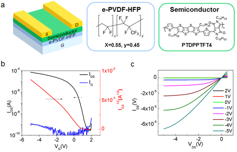
Figure 1. Chemical structure, device structure schematic and characterization of e-PVDF-HFP films.
(a) Transistor device structure and chemical structures of e-PVDF and PTDPPTFT4. (b,c) Output and transfer characteristics of PTDPPTFT4 (channel length L = 50 μm, channel width W = 1000 μm), where VDS = −5 V. The thickness of the dielectric is 1.4 μm. Two slopes in the IDS1/2 vs. VG plot were observed. This may be attributed to the existence of contact resistance in the device. We used the first slope in the range of +0.2 V to −2 V to estimate mobility values.

