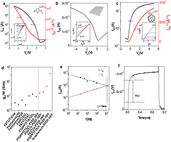
Figure 3. Electrical Characteristics of OTFTs based on e-PVDF-HFP dielectric layer with W/L = 20.
Transfer and output characteristics of the OTFTs of (a) P3HT, (b) graphene, and (c) PCBM, respectively. Note that the transfer characteristics of the graphene devices were evaluated in the linear-regime, where VDS = −0.1 V. Each panel exhibits the transfer curves with output characteristics shown in the inserted small figures. (d) Transconductance comparison between different dielectrics. All the transconductances were normalized to a driven gate voltage of −3 V. The black dots show the transconductance obtained from OFETs based on common dielectric layers, including cross-linked Cytop (d = 50–70 nm)34, cross-linked polystyrene (PS) (d = 10 nm)35, cross-linked poly(vinyl phenyl) (PVP) (thickness = 280 nm)36, SiO2 (d = 230–300 nm)37,38 and semicrystalline PVDF-HFP (thickness = 1.4 μm)39. Note that all SiO2 dielectrics were modified by OTS SAMs. The red dots represent the performance obtained from OFETs based on e-PVDF-HFP. The transconductances of all the e-PVDF-HFP devices are around one order of magnitude higher than the corresponding devices made on OTS-modified SiO2. (e) IDS and IG currents versus frequency of a PTDPPTFT4 transistor with e-PVDF-HFP as a dielectric layer (L = 50 μm, W = 1000 μm), where VDS = −15 V, VG = 10 V to −10 V. The cut-off frequency (fc) was estimated as the intersection of IDS and IG. (f) IDS response of PTDPPTFT4 to a square wavefunction gate-voltage pulse at 1 kHz, pulse width = 1 ms, pulse rise time = 4 μs, and channel length = 50 μm. The response time is defined as the time required to reach 80% of the maximum ON-current from 20% OFF.

