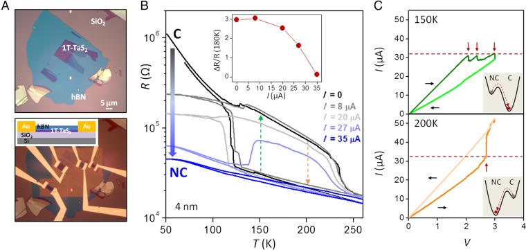
Fig. 2.
Electrical control of NC-C transition in oxidation-free, 2D devices. (A) Optical images of 1T-TaS2 flakes on a SiO2/Si wafer covered by hBN in inert atmosphere before (Upper) and after (Lower) side electrical contact. (Inset) Side-view device schematic. (B) ac resistance vs. temperature for 4-nm-thick device as a function of dc current. Continuous current flow stabilizes NC phase at low temperature. Normalized resistance difference between cooling and warming is plotted as a function of dc current in Inset. (C) (Upper) Current vs. voltage sweep at 150 K starting in NC phase shows abrupt decreases in current and transition to the C phase. (Lower) Same at 200 K starting in C phase shows abrupt increase in current and transition to NC phase. Sweep rate is 3–6 V/min. Free energy schematics of electrically induced transitions are plotted in Insets.

