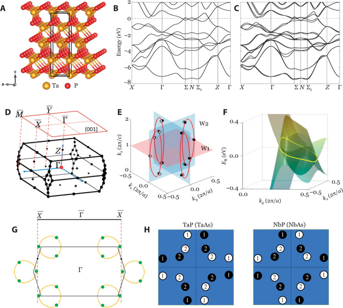
Fig. 1. Electronic band structure of the Weyl semimetal TaP.

(A) Body-centered tetragonal structure of TaP, shown as stacks of Ta and P layers. (B) First-principles band structure calculation of the bulk TaP without SOC. (C) Same as (B) but with SOC. Schematic of the distribution of Weyl nodes in the three-dimensional BZ of TaP. (D) Bulk BZ and (001) surface BZ of TaP, with certain high-symmetry points labeled. (E) Calculation of the positions of the Weyl nodes, with opposite chiralities indicated by the white and black circles. The mirror planes are blue and the kz = 2π/c plane is red. (F) Band structure on the kx = 0 mirror plane, E(kx = 0, ky, kz), in the vicinity of the ring-like crossing, in yellow, which we find in calculation when SOC is ignored. (G) Calculation showing the ring-like crossings in the kx = 0 plane, with the Weyl nodes indicated by green dots. The distribution of chiralities of the projected W1 nodes in the first surface BZ depends on whether the ring-like crossing is large enough that the W1 nodes spill over the edge of the first surface BZ, marked by the dotted line through the bulk N point. (H) To more clearly understand the distribution of chiralities, we show cartoons (not to scale) of the projected Weyl nodes and their chiral charges on the (001) Fermi surface of TaP (TaAs) and NbP (NbAs), respectively. The projected Weyl nodes are denoted by black and white circles; their color indicates their opposite chiralities and the number in the circle indicates the projected chiral charge. We find that the chiralities of the W1 points are swapped in TaP (TaAs) with respect to NbP (NbAs).
