
Figure 1. Schematic of microfluidic device fabrication and 3D cell encapsulation.
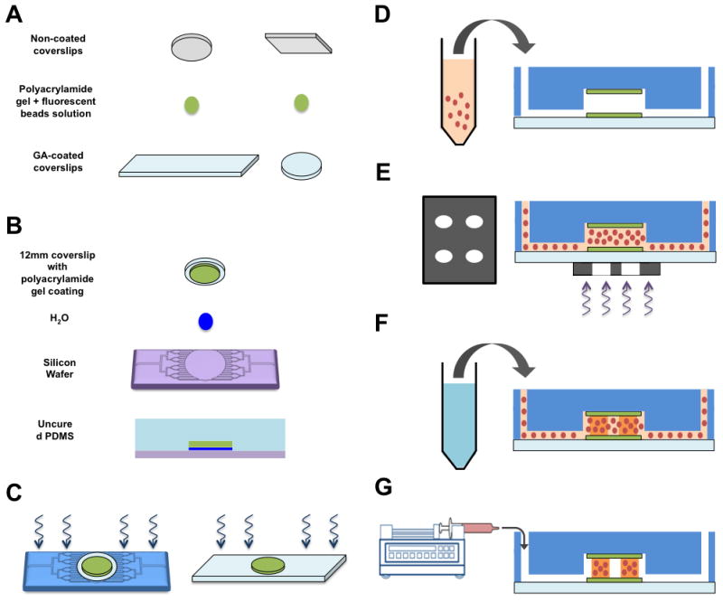
(A) Two PAm hydrogels were polymerized by sandwiching the precursor solution mixed with fluorescent nanoparticles between regular and GA-treated coverslips. (B) A small droplet of DI water was deposited onto a Teflon-coated silicon wafer prior to placing a PAm hydrogel tethered on a circular coverslip on top. PDMS solution containing the curing agent (10:1 ratio) was gently poured onto the construct and cured at 37 °C overnight. (C) The PDMS mold attached to the PAm hydrogel was removed from the wafer and inlet and outlet ports of the device were generated using a hole punch. This construct was bonded to a rectangular coverslip tethered to a PAm hydrogel using UV/Ozone treatment. Care was taken to align the two hydrogels during the process. The device was placed in 60°C for an hour within a humidity chamber prior to moving to a 37°C chamber overnight. (D) Cells mixed with GelMA, photoinitiator, and ascorbic acid were injected into the chamber. (E) A patterned transparency photomask was placed underneath the PAm hydrogels before exposing the region to UV light. (F) PBS solution was injected into the device to remove GelMA mixture in the non-polymerized region. (G) The device was attached to a syringe pump containing maintenance media to culture the cells encapsulated within patterned GelMA matrices.