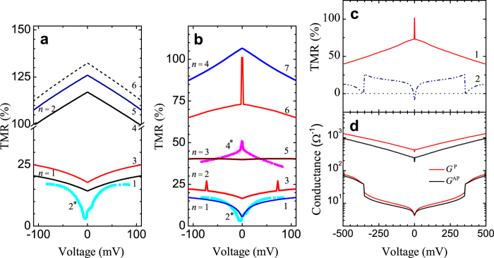
Figure 3.
(a) presents TMR-V simulations for d = 1.25 nm, kn=1 = 0.251 Å−1 and kn = 2 = 0.5026 Å−1, curves 1 (3) and 4 (5) correspond to kF,↑ = 1.09 (1.2) Å−1, respectively. The dashed curve 6 correspond to the magnetic state of NP with kF,↑ = 1.09 Å−1, kn=2,↑ = 0.5051 Å−1, kn=2,↓ = 0.5001 Å−1, other parameters see in the text; Curves 2* and 4* in (a,b) is experimental data11 for tNP = 0.45 nm and tNP = 1.2 nm, respectively (T = 2.5 K). (b) TMR curves 1, 3, 5–7 for the case of d = 2.6 nm correspond to the kn = 0.121, 0.242, 0.362, 0.4508, 0.483 Å−1, respectively. (c) Curve 1 shows peak-like TMR within extended voltage range and coincides with the curve 6 depicted in Fig. 3b, curve 2 shows negative TMR0 = −8% for kn = 0.115 Å−1, d = 2.6 nm. (d) Corresponding step-like quantized conductance is shown.

