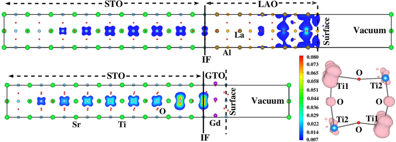
Figure 5. Conduction electron charge density for (LAO)5/(STO)9 (upper panel) and (GTO)1/(STO)9 (lower panel) in thin film-substrate geometry, integrated over an energy window from 0.1 eV below EF to EF.
The color of different contours corresponds to the values shown in the scale bar. The topmost AlO2 surface layer in LAO is metallic, while the topmost TiO2 layer in GTO is insulating. Inset: We also show the charge disproportionation with two inequivalent Ti sites on the top layer of GTO which drives the surface insulating. The charge density in this plot is obtained from integration over the lower Hubbard band in GTO; see text for details.

