Abstract
Libraries of nanostructured materials on a single chip are a promising platform for high throughput and combinatorial studies of structure-property relationships in the fields of physics and biology. Nanoporous gold (np-Au), produced by an alloy corrosion process, is a nanostructured material specifically suited for such studies because of its self-similar thermally induced coarsening behavior. However, traditional heat application techniques for the modification of np-Au are bulk processes cannot be used to generate a library of different pore sizes on a single chip. Here, laser micro-processing offers an attractive solution to this problem by providing a means to apply energy with high spatial and temporal resolution. In the present study we use finite element multiphysics simulations to predict the effects of laser mode (continuous-wave vs. pulsed) and thermal conductivity of the supporting substrate on the local np-Au film temperatures during photothermal annealing. Based on these results we discuss the mechanisms by which the np-Au network is coarsened. Thermal transport simulations predict that continuous-wave mode laser irradiation of np-Au thin films on a silicon substrate supports the widest range of morphologies that can be created through the photothermal annealing of np-Au. Using the guidance provided by simulations, we successfully fabricate an on-chip material library consisting of 81 np-Au samples of 9 different morphologies for use in the parallel study of structure-property relationships.
Keywords: nanoporous gold, thin film, nanostructure, photothermal annealing, laser micro-processing, thermal transport, surface diffusion, material library
Graphical Abstract
During the past decade, nanoscale materials have attracted significant interest for their unique structure-mediated properties. Structure-dependent optical, electrical, thermal, and mechanical properties make nanoscale materials promising candidates for use in applied devices as well as fundamental studies.1 In particular, porous metals have attracted much interest for applications in energy and biology research. One such emerging material is nanoporous gold (np-Au), which has many promising applications in electrochemical sensors,2-6 catalysis,2, 7 tunable molecular release,8-9 structure property studies at the nanoscale,6, 10-11 as well as biomaterial interfaces.12-14 Np-Au is produced through an alloy corrosion process known as dealloying,15 that generates a characteristic three dimensional nanoscale network of pores and ligaments. Microscopically, the porosity of np-Au develops by a kinetically-controlled self-organization process.15-16 The pore and ligament size distributions can be controlled through both altering dealloying parameters (i.e. temperature, time, and acid concentration) as well as post-fabrication annealing through the application of energy.17-20 Previous studies have demonstrated these morphology modification processes in both bulk (micrometer to millimeter-scale thickness) and thin film (nanometer-scale thickness) np-Au.2, 21-22 Here, we investigate a method for creating a library of varying np-Au morphologies on a single chip via precise delivery of tunable photothermal energy. More specifically, laser micro-processing (e.g. micromachining) provides the required spatial and temporal control imposing energy near the surface of the material, and already has long history as a highly controllable and precise method to cut, anneal, and modify materials.23-26 Inspired by recent work on laser-induced modification of ligament and pore size distributions of bulk np-Au,3, 21 the present study focuses on unique physical phenomena that arise during photothermal modification of supported thin films of np-Au . In contrast to bulk np-Au structures, np-Au thin films can be deposited and patterned by conventional microfabrication techniques, thereby exhibiting significant potential for facile integration into a plethora of applications. This paper reports on the effects of substrate properties and photothermal annealing parameters on the morphology evolution of np-Au thin films and utilizes this knowledge to engineer a material library of np-Au thin films that present varying morphologies. This report is organized to first provide an in depth theoretical analysis of the underlying essential physical mechanisms that constitute laser-mediated morphology evolution, secondly experimental validation of the simulated theoretical results, and finally fabrication of a single-chip material library.
Results and Discussion
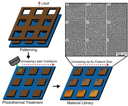
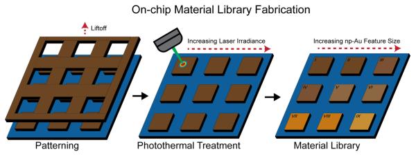
The successful fabrication of on-chip material libraries via laser-based photothermal treatment (Figure 1) requires extensive investigation into the effects of laser coupling to the nanostructured film and the resulting thermal profile. Laser-based photothermal annealing of np-Au thin films is accomplished through the local exposure and absorption of laser energy. This localized surface heating is caused primarily due to the absorption of photons by the material. Laser heating during annealing of non-porous surfaces has been extensively studied and generalized equations of the laser heating profile on many different materials have been reported.27-28 However, modeling laser heating on heat-sensitive nanostructured surfaces, such as np-Au, during the annealing process presents many challenging scenarios that must be considered.
Figure 1.
Schematic illustrating the suggested process to be used for the fabrication of on-chip np-Au (brown) material libraries supported on silicon or glass (blue) using laser-based precise photothermal treatment to selectively anneal each np-Au pattern, resulting in an altered feature size (denoted by color change) on each pattern.
Laser coupling to np-Au surface
At the foundation of photothermal heating of a material is the effectiveness of laser coupling to the material surface. The amount of energy that can be transferred to the material surface is determined by the efficiency of laser coupling to the material surface, commonly known as the absorptivity. Typically, absorptivity (Ab = 1 – Rb) of the bulk material, with Rb being material reflectivity, is used to linearly scale the power that is coupled to the material surface. The reflectivity of standard np-Au at a wavelength of λ = 532 nm has been calculated in previous studies as Rnp-Au = 0.22.21 However, as np-Au anneals due to heating, the reflectivity approaches the value of planar Au given by Rpl-Au = 0.62.29 This increase in reflectivity during laser exposure can potentially account for up to a 40% decrease in laser energy being transferred into the np-Au film during photothermal treatment. However, to our knowledge no comprehensive models exist to accurately predict changes in np-Au reflectivity during thermal coarsening. Taking into account a full shift of reflectivity to that of planar Au results in a decrease in maximum film temperature of approximately 35-40% for CW and 56% for pulsed (Figure S5). Since the np-Au morphologies studied in this work are still notably porous, the previously reported reflectivity value for untreated np-Au was used to calculate an absorptivity value in the following models. Additionally, since a shift in the reflectivity towards that of planar Au causes less heating of the film (Figure S5), we consider that the modeled coupling in this study (retaining np-Au reflectivity) is the scenario of maximal energy transfer to the film.
Heat transfer in the np-Au film
In order to model heat transfer in the np-Au film due to laser-induced surface heating, the thermal conductivity of np-Au, κnp-Au, must be determined. The thermal conductivity of np-Au and the effect of thermal treatment on the thermal conductivity has been studied previously.30-31 Here, we use the calculations performed by Hopkins et al. to calculate the thermal conductivity of the np-Au film.31 Briefly, this method uses the product of two scaling ratios to determine the conductivity of np-Au at a given ligament diameter. The ligament diameters of the np-Au films used in this study are on the order of 50 nm, as reported previously by our group.12, 22 First, the ratio of the reduced conductivity due to ligament diameter, κw, to the bulk conductivity, κb, is calculated by
where u is the ratio of the ligament diameter to the electron mean free path in the ligament. A value of u is found to be approximately 1.1 assuming a ligament diameter of 50 nm and the electron mean free path of 45 nm. It is worth noting that this equation is only valid for values of u > 1. Using bulk conductivity, κb, of Au (317 W m−1 K−1) the reduced conductivity κw in as-deposited films is found to be 190.2 W m−1 K−1. Next, the decrease in conductivity due to the presence of pores is calculated using the equation
where f is the porosity and κp is the final thermal conductivity of np-Au (κnp-Au). Using a porosity of 50% for the films used in this study, approximated by taking into account elemental composition before/after dealloying (64% to 3-5%) and percent film shrinkage after dealloying (~12%), a value of 67.14 W m−1 K−1 is determined for np-Au thermal conductivity. Subsequent analysis for larger 200 nm diameter ligaments (thermally coarsened) reveals an increase in np-Au thermal conductivity to 95.12 W m−1 K−1 (41.6% increase). This suggests that, as for the case of reflectivity, the thermal conductivity also increases during annealing. Simulations (Figure S6) demonstrate this increase in thermal conductivity accounts for a decrease in maximum film temperature of approximately 12% for CW and 33% for pulsed. However, since this system consists of a thin 600 nm np-Au film and a thick 500 μm supporting material, the heat transport in the system is dominated by thermal flux into the supporting material and not laterally through the np-Au film, resulting in no drastic changes to the heating profile (Figure S6 A,C,E).
The laser mode used for photothermal treatment is another important factor determining the temporal temperature profile that controls the extent of thermally induced coarsening. The laser energy can be applied through either a continuous-wave (CW) or pulsed mode laser beam. Typically, CW irradiation is used in applications where extended heating and steady application of energy is needed, whereas pulsed lasers are used extensively in applications involving ablation due to the rapid (nanosecond to femtosecond) and intense (~GW/cm2) energy deposition precisely limiting the extent of excess thermal damage. Finally, the absorbed laser irradiance can be modeled as a Gaussian heat source boundary condition to obtain the heating profile in the film. In order to accurately model the Gaussian profile of the beam the power was scaled as a function of the ratio of radial beam intensity to maximum intensity given by,
where r corresponds to the radial position relative to the center of the Gaussian laser beam and d to the laser spot 1/e2 diameter.
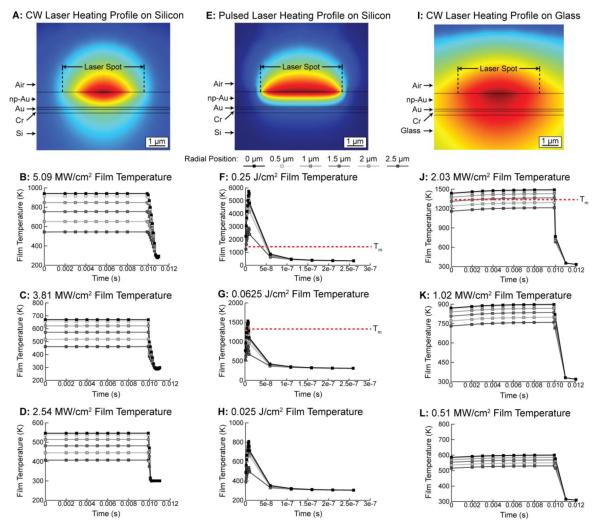
In order to investigate both the temporal and spatial film temperature distribution as a function of laser mode, COMSOL, a finite element multiphysics modeling program, was used to create a model simulating the application of both laser modes using parameters seen in the supporting information (Figure S1 & Table S1). Simulations were performed at irradiances of Ecw = 5.09 MW/cm2, 3.81 MW/cm2, and 2.54 MW/cm2 for the CW mode as well as fluences of Ep = 0.25 J/cm2, 0.0625 J/cm2 and 0.025 J/cm2 for pulsed mode. These powers correspond to 80%, 60%, and 40% of maximum operating power for CW, whereas the pulse energies used correspond to 1%, 0.25%, and 0.1% power for the pulsed mode. Film temperatures from this model were taken at 6 points (0, 0.5, 1, 1.5, 2, and 2.5 μm) along the Gaussian profile of the surface heating. These film temperatures represent the maximum temperatures in the np-Au film over the radial distribution of the laser beam.
A comparison between CW and pulsed mode laser irradiation on silicon reveals distinctly different heat transport through the np-Au film (Figure 2 A & E) and temperature profiles (Figure 2 B-D & F-H). The main reason for this difference is the duration of energy application, 10 ms for CW exposure vs. 9 ns for pulsed exposure. The long exposure time of CW irradiation allows for adequate thermal diffusion time and maintains the film at a steady state temperature for the majority of the treatment duration. Conversely, the extremely short exposure time of the pulsed irradiation leads to a spike in film temperature with too short of a thermal diffusion time to reach steady state. This is an important difference as surface diffusion is a relatively slow process that requires time to result in meaningful coarsening. Another key difference between irradiation in CW and pulsed modes (at least for the systems used in this study) is the large difference between energy densities of the laser systems. At 5.09 MW/cm2 (80% system power) the CW laser irradiation maintains steady state film temperatures across the entire radial beam distance that are under the melting point of Au (Tm = 1337 K), whereas at 0.25 J/cm2 (1% system power) pulsed laser irradiation increases the film temperature to more than four times the melting temperature of Au. Decreasing the pulsed laser energy density to 0.025 J/cm2 (0.1% system power) is required to maintain film temperatures in a regime similar to that of 5.09 MW/cm2 CW mode irradiation. This result is not surprising and is an essential reason for pulsed mode lasers to be typically used for cutting applications due to the fast delivery of high energy density irradiation while maintaining low thermal damage due a long duration between pulses.
Figure 2.
Simulated heat distribution in np-Au film in response to CW (A) and pulsed (E) laser irradiation on silicon as well as CW irradiation on glass (I). Resulting film temperature profiles are shown for 5.09 MW/cm2 (B), 3.81 MW/cm2 (C), 2.54 MW/cm2 (D) for the CW mode on silicon, 0.25 J/cm2 (F), 0.0625 J/cm2 (G), 0.025 J/cm2 (H) for the pulsed mode on silicon and 2.03 MW/cm2 (J), 1.02 MW/cm2 (K), 0.51 MW/cm2 (L) and glass respectively. A red dashed line denotes the melting temperature (1337 K) of bulk Au.
Previously, studies on photohermal annealing of np-Au used thick (200 μm) unsupported disks and therefore did not need to account for temperature differences in the film due to underlying substrate. Using glass, instead of silicon, as the supporting substrate decreases the thermal conductivity relative to Si from 149 W m−1 K−1 to 1.47 W m−1 K−1 – approximately a hundred-fold decrease in conductivity. The simulations demonstrate that changing the supporting substrate from a thermally conductive material (silicon) to a less thermally conductive material (glass) drastically alters heat transport in the film. In glass-supported films, heat does not get transported into the bulk supporting material as readily causing heat accumulation in the area under and surrounding the laser spot (Figure 2 I). This effect increases the film temperatures far beyond what is seen in films supported on silicon. Even with a 2.5-fold reduction in laser irradiance at 2.03 MW/cm2, the glass substrate causes the np-Au film to reach temperatures above the melting point of Au. However, lower irradiances of 1.02 MW/cm2 and 0.51 MW/cm2 reach a steady state value below the melting temperature of Au. This suggests that in changing the thermal conductivity of the supporting substrate, the range of irradiance needed to control the annealing of np-Au is shifted to a lower and narrower range. Additionally, unlike np-Au film on a silicon substrate, the np-Au film on glass takes a longer time to reach a steady state temperature (Figure 2 J-L), which underlies the characteristic heat accumulation in the film due to lack of a highly conductive sink material. In all simulations film cooling occurs fast enough that negligible annealing can happen after laser irradiation. Here, we simulated the heat transfer in thin film np-Au under multiple model conditions of changing laser mode and substrate thermal conductivity. This enables the investigation of the dominant np-Au film coarsening mechanisms during photothermal annealing.
Mechanisms of mass transport in np-Au film during photothermal annealing
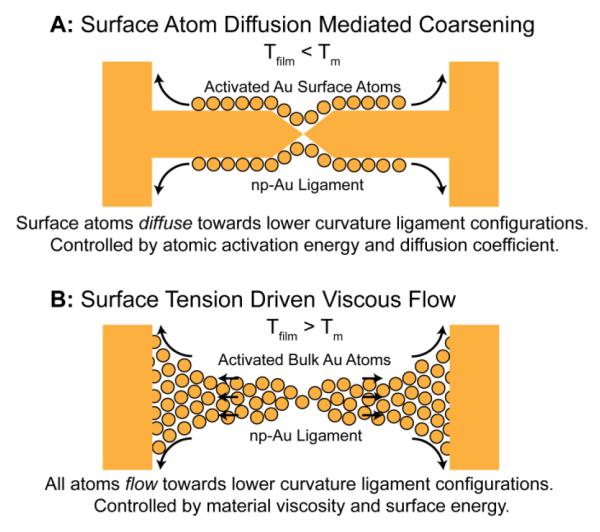
The coarsening of np-Au can primarily happen through two mechanisms: (i) curvature-driven surface diffusion for temperatures below the melting temperature and (ii) surface tension-driven viscous flow for temperatures above the melting point (Figure 3). For the purpose of creating controllable np-Au morphologies, coarsening through surface diffusion is the desired mechanism because it provides superior feature size control through controlling the diffusion kinetics and results in a self-similar structure. Melting, by contrast, is a first order phase transition causing abrupt mass transport property changes.
Figure 3.
Diagram illustrating surface atom diffusion-mediated coarsening (A) and surface tension-driven viscous flow (B).
Because surface diffusion is a relatively slow process, appreciable coarsening of the material via surface diffusion requires that the local temperatures are raised by several hundred degrees and maintained below the melting temperature of Au for at least multiple milliseconds. Therefore, it is essential to identify process parameters that achieve elevated (but below the melting temperature of Au) local temperature profiles on the millisecond time scale.
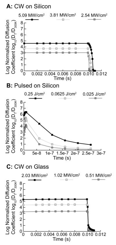
The simulations reveal that both CW and pulsed mode laser heating for the conditions discussed above result in film temperatures below the melting point with the exception of 2.03 MW/cm2 CW mode on glass and the 0.25 J/cm2 pulsed mode exposure (Figure S3). However, the exposure time depends drastically on the laser operating mode with CW heating resulting in six orders of magnitude longer exposures than pulsed mode. Using the simulated temperatures, it is possible to estimate diffusion coefficient of surface atoms, which plays the central role in coarsening illustrated in Figure 3A. The surface diffusion coefficient of Au has been characterized previously32 to follow an Arrhenius relationship with the temperature of the material given by
where Do is a pre-exponential factor empirically determined to be 5 × 10⁻¹² m2 s−1, EA is the activation energy of gold 0.4 eV, kb is the Boltzmann constant, and T is the temperature of the material. Using this equation, the diffusion coefficient can be determined as a function of changing film temperature over time (Figure 4).
Figure 4.
Log10 of the normalized diffusion coefficient over the time course of photothermal annealing at r = 0 μm for each simulated case demonstrates distinct differences between the temporal activation of the np-Au film.
Clearly, only CW exposure results in sufficiently high (and stable) diffusion coefficients over sufficiently long times to allow for appreciable coarsening. On the other hand, in all but one case the pulsed laser reaches temperatures above the melting temperature of bulk Au leading to viscous flow rather than surface diffusion mediated thermal coarsening. Additionally, the associated time-scale for the pulsed mode is much too short to allow for appreciable coarsening, even at film temperatures close to the melting point of bulk Au. Although there is no simple relationship between the surface diffusion coefficient or characteristic diffusion length and resulting film morphology, there is a monotonic relationship where increased diffusion length () manifests itself as coarser morphologies. The diffusion lengths in Table 1 are calculated by taking the square root of the integral of diffusion coefficients in Figure 3 for the treatment duration. These calculations demonstrate the difference between CW and pulsed mode laser irradiation for the efficacy of surface diffusion-mediated thermal coarsening in np-Au films.
Table 1.
Characteristic diffusion length values and maximum film temperatures for each simulated laser mode and substrate
| CW on silicon | Diffusion Length | Maximum Film Temperature |
|---|---|---|
| 5.09 MW/cm2 | 59.18 nm | 941 K |
| 3.81 MW/cm2 | 20.01 nm | 670 K |
| 2.54 MW/cm2 | 9.12 nm | 546 K |
| CW on glass | ||
| 2.03 MW/cm2 | 130.64 nm | 1490 K |
| 1.01 MW/cm2 | 47. 58 nm | 898 K |
| 0.51 MW/cm2 | 13.24 nm | 600 K |
| Pulsed on silicon | ||
| 0.25 J/cm2 | 0.42 nm | 5732 K |
| 0.0625 J/cm2 | 0.11 nm | 1533 K |
| 0.025 J/cm2 | 0.026 nm | 807 K |
The sub-nanometer values obtained for the pulsed laser suggest that any annealing that is observed during photothermal treatment would need to be dominated by viscous flow and not surface atom diffusion. Therefore it is very unlikely that pulsed mode laser irradiation can result in subtle morphological changes, but rather causes rapid flow of molten Au towards larger structures – an interesting result but not amenable to engineering morphology libraries.
Morphology and analysis of photothermally annealed np-Au films
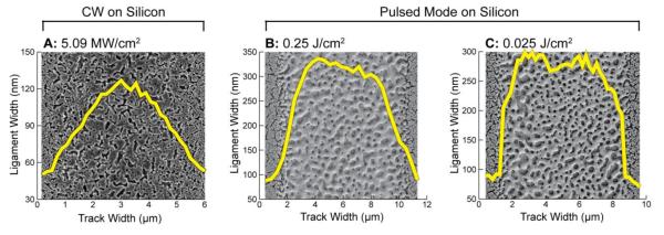
Guided by the simulation results, np-Au thin films with thicknesses similar to those used in the simulations were fabricated on both silicon and glass supporting substrates. These samples were then annealed by either CW or pulsed mode laser irradiation using a custom set-up for CW mode (Figure S2) and a New Wave Research (Fremont, CA) laser mill for pulsed mode irradiation. The resulting np-Au morphologies, studied by scanning electron microscopy (SEM), differ significantly for the different annealing parameters, most notably between CW and pulsed mode annealing. The morphology changes were analyzed through a custom MATLAB script that calculated the average ligament width over the track width. Large changes in the coarsening distributions (superimposed on SEMs) are seen in pulsed mode compared to the CW mode (Figure 5).
Figure 5.
Scanning electron micrographs of np-Au thin films on silicon, that are photothermally annealed by CW (A) and pulsed (B & C) mode laser irradiation. Images reveal the differences in ligament size over the width of the irradiation tracks between the two modes.
As expected from the previous analysis, 0.25 J/cm2 pulsed mode irradiation (Figure 5 B) leads to local melting of the np-Au film rather than controllable coarsening as seen for 5.09 MW/cm2 CW irradiation (Figure 5 A). Interestingly, the lower pulsed energy density used in the simulations (0.025 J/cm2) also led to complete melting of the np-Au film contrary to the simulation that predicted film temperatures well below the melting temperature of Au. This can be explained by the power range of the pulsed laser system used for this study. At 0.025 J/cm2 the system is running at 0.1% of the full power, which likely results in poor control over the applied power. Given the diffusion length analysis (Table 1), it is however highly unlikely the short pulse duration can produce any meaningful coarsening of the np-Au film. To achieve appreciable surface diffusion mediated coarsening of np-Au with a pulsed mode laser would require combining very high pulse repetition rates with extremely low power density, which essentially converges the pulsed mode to CW mode. Additional analysis of the viscous and diffusion related rearrangement of np-Au was done using frequency spectrum analysis to fit an analytical model of surface smoothing33 and is shown in the supporting information (Figure S4).
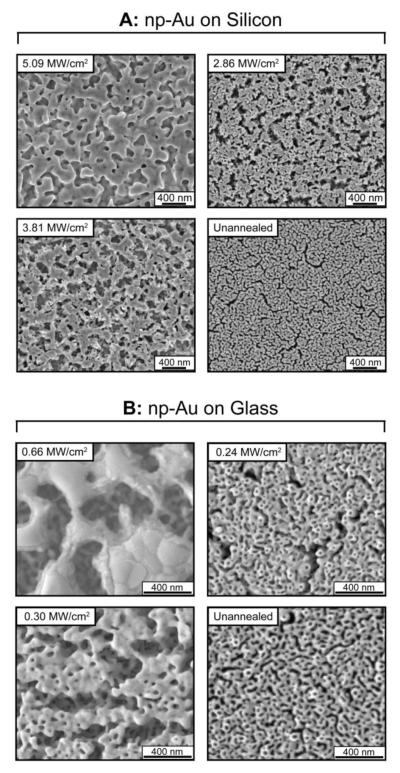
Investigating the effect of substrate thermal conductivity yields results consistent with the simulations, with the irradiance range that leads to controlled morphology changes being much smaller for glass (0.66 MW/cm2 to 0.24 MW/cm2) than for silicon substrates (5.09 MW/cm2 to 2.54 MW/cm2). Interestingly, the range of irradiance determined experimentally for the glass substrate was approximately 25% lower than the simulated irradiance where the np-Au film temperatures were indicative of np-Au coarsening (Figure 6).
Figure 6.
Np-Au thin film coatings supported on both silicon (A) and glass (B) demonstrate drastically different ranges of irradiance needed for control over np-Au morphology through photothermal annealing.
This can be explained by differences in the glass used experimentally and in the simulations resulting in an even lower thermal conductivity of the glass during these experiments. Regardless, this result clearly demonstrates that silicon as a substrate enables the widest range of powers to be used to create multiple morphologies of np-Au. Now that the supporting substrate and laser mode have been selected np-Au material libraries of morphologies on a single chip can be fabricated using precise photothermal annealing.
Material library fabrication
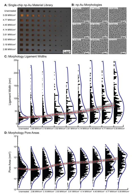
Guided by our simulations and preliminary experimental data, we fabricated a material library on a single chip that consists of microfabricated np-Au thin film patterns individually coarsened to present different morphologies. A 9 by 9 array of 81 different np-Au squares ranging from 1 mm2 to 0.04 mm2 was fabricated onto a single 20 mm square silicon chip (Figure 7 A). Each chip was then annealed using a fully automated LabVIEW script with decreasing laser irradiance per row. Starting at Ecw = 5.09 MW/cm2 and decreasing to Ecw = 2.86 MW/cm2 by the final row, with a constant stage velocity of 500 μm/s and beam diameter of 5 μm. The entire surface was annealed through rastering of the laser across the np-Au surface with raster spacing starting at 5 μm (Ecw = 5.09 MW/cm2) and ending at 2.5 μm (Ecw = 2.86 MW/cm2). This decrease in raster spacing is necessary to account for the decreasing irradiance input from the laser, and therefore the decreasing effective laser spot size, to ensure uniform annealing across the entire np-Au surface. After annealing, each square on the material library was imaged and characterized for changes in both ligament width and pore diameter (Figure 7 C & D).
Figure 7.
(A) 9 × 9 array of np-Au patterns on single 20 mm silicon chip. Each column contains 9 identical squares spaces 1 mm apart with each row decreasing height and width by 100 μm starting at 1 mm height and width (far left) and decreasing to 200 μm height and width (far right). (B) Top-view SEM images of each photothermally annealed np-Au morphology on the np-Au material library. (C) Ligament width analysis demonstrates a roughly linear increase in ligament width as laser irradiance is increased. (D) Pore area analysis demonstrates a clear increase in pore size with increasing laser powers, with distributions becoming less dominantly distributed towards smaller pore areas. Red dashed line denotes median value for both ligament width and pore area distributions and the surrounding shaded region corresponds to the standard error.
The morphologies created on the material library show a roughly linear dependence between ligament widths and pore area versus laser irradiance (Figure 7 C & D). This is an expected result due to the generally linear dependence between the film temperature and applied laser power for the photothermal annealing process. Interestingly, the distributions of ligament width and pore area are altered differently through the process of annealing. The ligament size distribution, originally skewed toward small ligaments, spreads upwards during the process of annealing. This is indicative of ligaments joining and creating larger ligaments in smaller numbers (Figure 7 C). On the other hand, the entire pore area distribution shifts towards a larger pore area first becoming a multimodal distribution of a small and large dominant pore area before shifting almost entirely to the larger dominant pore area. (Figure 7 D).
Conclusion
In conclusion, here we have laid out the framework for successful understanding and simulation of the photothermal annealing process for thin film porous materials through investigating laser material coupling, heat distribution in the film, and the underlying mechanisms of coarsening in the film. Through this analysis we have demonstrated that continuous-wave irradiation is a superior method for driving surface atom diffusion-dominated coarsening while pulsed mode irradiation drives bulk viscous flow of the material. Additionally, we have demonstrated that supporting substrate thermal conductivity plays a crucial role in determining the controllability of the obtainable np-Au morphologies. This has important implications in the fabrication of electrically addressable material libraries. Finally, we have shown that for np-Au, precision photothermal annealing through the application of a CW (λ = 532 nm) laser effectively controls ligament width and pore diameter changes of np-Au coatings on silicon substrates. This method has been used to create np-Au material libraries consisting of several different morphologies on a single chip. These libraries have the potential to drastically increase the throughput of morphology interaction studies for np-Au specifically in applications such as surface enhanced Raman spectroscopy (SERS),34 high capacity lithium ion batteries,35 cell-material interaction studies for neural interfaces,12, 36 analytical biosensors,37 as well as nanoscale material science studies.38 Further optimization of both the material selection (i.e. selecting insulting layers with higher thermal conductivity) and laser parameters (i.e. stable low operating power) is currently underway in order to produce multiple electrode array material libraries. Ultimately this work sets the foundation for understanding laser-based annealing of porous thin film materials and with the fabrication of single chip material libraries has the potential to increase the throughput of material interaction testing in many disciplines through easy single-chip material screening libraries.
Methods
Sample fabrication and characterization
5 mm-diameter spots of thin films of gold-silver alloy were deposited onto the middle of a piranha-cleaned 12 mm-diameter thin (0.15 mm thick) glass slide or onto a bare or lithographically-patterned silicon wafer. Gold-silver alloy films (precursor to np-Au) were deposited by direct current sputtering (Kurt. J. Lesker) of a 600 nm-thick gold and silver alloy film (64% silver and 36% gold; atomic %) on top of 80 nm-thick gold corrosion barrier and 50 nm-thick chromium adhesion layer. The np-Au films were obtained by immersing the gold-silver alloy in heated (55°C) nitric acid (70%) for 15 minutes. The short dealloying times used in the present study typically result in residual silver levels in the order of 3-5%.8, 13 The samples were then soaked in deionized (DI) water for 24 hours before drying under nitrogen flow. Caution: Nitric acid is highly corrosive and reactive with organic materials and must be handled with extreme care. The morphology of the coatings was characterized by scanning electron microscopy (FEI Nova NanoSEM430), and elemental compositions before and after dealloying were assessed with energy dispersive X-ray spectroscopy (Oxford INCA, Energy-EDS). Average ligament width was analyzed using a custom MATLAB script by averaging both vertically and horizontally over each SEM image taken. Pore area was calculated through a custom contour finding program written in Python.
Photothermal annealing of np-Au films
Photothermal laser annealing was carried out either with a continuous-wave (CW) laser (experimental set-up shown in Figure S2) or a pulsed laser mill (New Wave Research, Fremont, CA). In the CW mode set-up, a CW laser (SproutD, Lighthouse Photonics) operating at a wavelength of λ = 532 nm was focused in 5 μm spot onto the sample through a 5X objective (Mitutoyo M Plan Apo 5x). Samples were mounted on a motorized XY stage (ASI MS2000) with manual Z axis control for focus. The stage allows for movement in a 100 mm range in both the X and Y directions at a speed up to 7 mm/s (500 μm/s used for this study). Stage, laser, shutter, and camera control was accomplished through a self-written LabVIEW control program that enables the complete automation of the laser processing.
Fabrication of np-Au single chip material libraries
Np-Au material libraries were fabricated on a single chip through traditional microfabrication photolithography, deposition, and lift-off stages all performed at the Center for Nano and Micro-manufacturing clean room at the University of California, Davis. Briefly, silicon wafers (University Wafer) were spun with ~2 μm of AZ 5214E-IR (Clariant) and patterned using a film mask. Alloy deposition was carried out as per the previously mentioned protocol. After deposition photoresist was lifted through exposure to N-Methyl-2-pyrrolidone (NMP) for ~4 hours.
Supplementary Material
Acknowledgements
We gratefully acknowledge the support from a UC Lab Fees Research Program Award [12-LR-237197] and a Research Investments in the Sciences & Engineering (RISE) Award. C. Chapman was supported by a National Science Foundation Graduate Research Fellowship [DGE-1148897] and a predoctoral fellowship from the National Institutes of Health [T32-GM008799]. Any opinion, findings, and conclusions or recommendations expressed in the material are those of the authors(s) and do not necessarily reflect the views of the National Science Foundation or the National Institutes of Health. Work at LLNL was performed under the auspices of the U.S. DOE by LLNL under Contract DE-AC52-07NA27344.
Footnotes
Details of sample preparation, fabrication of material libraries, as well as further analysis and supporting scanning electron micrographs can be found in Supporting Information. This material is available free of charge via the Internet at http://pubs.acs.org
Author Contributions
The manuscript was written through contributions of all authors. All authors have given approval to the final version of the manuscript.
References
- 1.Gleiter H. Nanostructured Materials: Basic Concepts and Microstructure. Acta Materialia. 2000;48:1–29. [Google Scholar]
- 2.Seker E, Reed ML, Begley MR. Nanoporous Gold: Fabrication, Characterization, and Applications. Materials. 2009;2:2188–2215. [Google Scholar]
- 3.Santos GM, Zhao F, Zeng J, Shih W. Characterization of Nanoporous Gold Disks for Photothermal Light Harvesting and Light-Gated Molecular Release. Nanoscale. 2014;6:5718–5724. doi: 10.1039/c4nr01266f. [DOI] [PubMed] [Google Scholar]
- 4.Li K, Huang J, Shi G, Zhang W, Jin L. A Sensitive Nanoporous Gold-Based Electrochemical DNA Biosensor for Escherichia Coli Detection. Anal. Lett. 2011;44:2559–2570. [Google Scholar]
- 5.Feng J, Zhao W, Wu J. A Label-Free Optical Sensor Based on Nanoporous Gold Arrays for the Detection of Oligodeoxynucleotides. Biosens. Bioelectron. 2011;30:21–27. doi: 10.1016/j.bios.2011.08.021. [DOI] [PubMed] [Google Scholar]
- 6.Jin HJW, J. A Material with Electrically Tunable Strength and Flow Stress. Science. 2011;332:1179–1182. doi: 10.1126/science.1202190. [DOI] [PubMed] [Google Scholar]
- 7.Fujita T, Guan P, McKenna K, Lang X, Hirata A, Zhang L, Tokunaga T, Arai S, Yamamoto Y, Tanaka N, Ishikawa Y, Asao N, Yamamoto Y, Erlebacher J, Chen M. Atomic Origins of the High Catalytic Activity of Nanoporous Gold. Nat. Mater. 2012;11:775–780. doi: 10.1038/nmat3391. [DOI] [PubMed] [Google Scholar]
- 8.Kurtulus O, Daggumati P, Seker E. Molecular Release from Patterned Nanoporous Gold Thin Films. Nanoscale. 2014;6:7062–7071. doi: 10.1039/c4nr01288g. [DOI] [PubMed] [Google Scholar]
- 9.Gittard S, Pierson B, Ha C, Wu C, Narayan R, Robinson D. Supercapacitive Transport of Pharmacologic Agents Using Nanoporous Gold Electrodes. Biotechnol. J. 2010;5:192–200. doi: 10.1002/biot.200900250. [DOI] [PubMed] [Google Scholar]
- 10.Hodge AM, Hayes JR, Caro JA, Biener J, Hamza AV. Characterization and Mechanical Behavior of Nanoporous Gold. Adv. Eng. Mater. 2006;8:853–857. [Google Scholar]
- 11.Lee D, Wei X, Chen X, Zhao M, Jun SC, Hone J, Herbert EG, Oliver WC, Kysar JW. Microfabrication and Mechanical Properties of Nanoporous Gold at the Nanoscale. Scr. Mater. 2007;56:437–440. [Google Scholar]
- 12.Chapman CAR, Chen H, Stamou M, Biener J, Biener MM, Lein PJ, Seker E. Nanoporous Gold as a Neural Interface Coating: Effects of Topography, Surface Chemistry, and Feature Size. ACS Appl. Mater. Interfaces. 2015 doi: 10.1021/acsami.5b00410. [DOI] [PMC free article] [PubMed] [Google Scholar]
- 13.Seker E, Berdichevsky Y, Begley MR, Reed ML, Staley KJ, Yarmush ML. The Fabrication of Low-Impedance Nanoporous Gold Multiple-Electrode Arrays for Neural Electrophysiology Studies. Nanotechnology. 2010;21:1–7. doi: 10.1088/0957-4484/21/12/125504. [DOI] [PMC free article] [PubMed] [Google Scholar]
- 14.Seker E, Berdichevsky Y, Staley KJ, Yarmush ML. Microfabrication-Compatible Nanoporous Gold Foams as Biomaterials for Drug Delivery. Adv. Healthcare Mater. 2012;1:172–176. doi: 10.1002/adhm.201200002. [DOI] [PMC free article] [PubMed] [Google Scholar]
- 15.Erlebacher J, Aziz MJ, Karma A, Dimitrov N, Sieradzki K. Evolution of Nanoporosity in Dealloying. Nature. 2001;410:450–453. doi: 10.1038/35068529. [DOI] [PubMed] [Google Scholar]
- 16.Hakamada MM, M. Thermal Coarsening of Nanoporous Gold: Melting or Recrystallization. J. Mater. Res. 2008;24:301–304. [Google Scholar]
- 17.Forty AJD, P. A Micromorphological Study of the Dissolution of Silver-Gold Alloys in Nitric Acid. Philos. Mag. A. 1980;42:295–318. [Google Scholar]
- 18.Qian LHC, M. W. Ultrafine Nanoporous Gold by Low-Temperature Dealloying and Kinetics of Nanopore Formation. Appl. Phys. Lett. 2007;91:083105-1–083105-3. [Google Scholar]
- 19.Li RS, K. Ductile-Brittle Transition in Random Porous Au. Phys. Rev. Lett. 1992;68:1168–1171. doi: 10.1103/PhysRevLett.68.1168. [DOI] [PubMed] [Google Scholar]
- 20.Hakamada MM, M. Microstructural Evolution in Nanoporous Gold by Thermal and Acid Treatments. Mater. Lett. 2008;62:483–486. [Google Scholar]
- 21.Schade L, Franzka S, Mathieu M, Biener MM, Biener J, Hartmann N. Photothermal Laser Microsintering of Nanoporous Gold. Langmuir. 2014;30:7190–7197. doi: 10.1021/la5011192. [DOI] [PubMed] [Google Scholar]
- 22.Dorofeeva TSS, E. Electrically-Tunable Pore Morphology in Nanoporous Gold Thin Films. Nano Res. 2015 [Google Scholar]
- 23.Matthews MJ, Yang ST, Shen N, Elhadj S, Raman RN, Guss G, Bass IL, Nostrand MC, Wegner PJ. Micro-Shaping, Polishing, and Damage Repair of Fused Silica Surface Using Focused Infrared Laser Beams. Adv. Eng. Mater. 2014;17:247–252. [Google Scholar]
- 24.Elhadj S, Matthews MJ, Yang ST. Combined Infrared Thermal Imaging and Laser Heating for the Study of Materials Thermophysical and Processing Properties at High Temperatures. Critical Reviews in Solid State and Materials Sciences. 2014;39:175–196. [Google Scholar]
- 25.Guss GM, Sridharan AK, Elhadj S, Johnson MA, Matthews MJ. Nanoscale Surface Tracking of Laser Material Processing Using Phase Shifting Diffraction Interferometry. Optics Express. 2014;22:14493–14504. doi: 10.1364/OE.22.014493. [DOI] [PubMed] [Google Scholar]
- 26.Schade L, Franzka S, Hardt S, Wiggers H, Hartmann N. Sintering of Thin Titanium Dioxide Nanoparticle Films Via Photothermal Processing with Ultraviolet Continuous-Wave Lasers. Appl. Surf. Sci. 2013;278:336–340. [Google Scholar]
- 27.Lax M. Temperature Rise Induced by a Laser Beam. J. Appl. Phys. 1977;48:3919–3924. [Google Scholar]
- 28.Bauerle D. Laser Processing and Chemistry. Springer; Berlin: 2000. [Google Scholar]
- 29.Schroter A, Kalus M, Hartmann N. Substrate-Mediated Effects in Photothermal Patterning of Alkanethiol Self-Assembled Monolayers with Microfocused Continuous-Wave Lasers. Bielstein J. Nanotechnol. 2012;3:65–74. doi: 10.3762/bjnano.3.8. [DOI] [PMC free article] [PubMed] [Google Scholar]
- 30.Wang J, Xia R, Zhu J, Ding Y, Zhang X, Chen Y. Effect of Thermal Coarsening on the Thermal Conductivity of Nanoporous Gold. J. Mater. Sci. 2011;47:5013–5018. [Google Scholar]
- 31.Hopkins PE, Norris PM, Phinney LM, Policastro SA, Kelly RG. Thermal Conductivity in Nanoporous Gold Films During Electron-Phonon Nonequilibrium. J. Nanomater. 2008;2008:7. [Google Scholar]
- 32.Gobel H. v. B., P. A Study of Surface Diffusion on Gold with an Atomic Force Microscope. Surf. Sci. 1995;331:885–890. [Google Scholar]
- 33.Cassidy DCG, N. A. Capillarity-Induced Smoothing of Glass Surfaces by Viscous Flow. J. Am. Ceram. Soc. 1969;53:161–168. [Google Scholar]
- 34.Bianco GV, Giangregorio MM, Losurdo M, Capezzuto P, Bruno G. Supported Faceted Gold Nanoparticles with Tunable Surface Plasmon Resonance for Nir-Sers. Adv. Func. Mater. 2012;22:5081–5088. [Google Scholar]
- 35.Ye J, Baumgaertel AC, Wang YM, Biener J, Biener MM. Structural Optimization of 3d Porous Electrodes for High-Rate Performance Lithion Ion Batteries. ACS Nano. 2015;9:2194–2202. doi: 10.1021/nn505490u. [DOI] [PubMed] [Google Scholar]
- 36.Tan YH, Terrill SE, Paranjape GS, Stine KJ, Nichols MR. The Influence of Gold Surface Texture on Microglia Morphology and Activation. Biomater. Sci. 2014;2:110–120. doi: 10.1039/c3bm60096c. [DOI] [PubMed] [Google Scholar]
- 37.Daggumati P, Matharu Z, Seker E. Effect of Nanoporous Gold Thin Film Morphology on Electrchemical DNA Sensing. Anal. Chem. 2015 doi: 10.1021/acs.analchem.5b00846. [DOI] [PubMed] [Google Scholar]
- 38.Biener MM, Biener J, Wang YM, Shin SJ, Tran IC, Willey TM, Perez FN, Poco JF, Gammon SA, Fournier KB, van Buuren AW, Statcher JH, Hamza AV. Atomic Layer Deposition-Derived Ultra-Low-Density Composite Bulk Materials with Deterministic Density and Composition. ACS Appl. Mater. Interfaces. 2013;5:13129–13134. doi: 10.1021/am4041543. [DOI] [PubMed] [Google Scholar]
Associated Data
This section collects any data citations, data availability statements, or supplementary materials included in this article.


