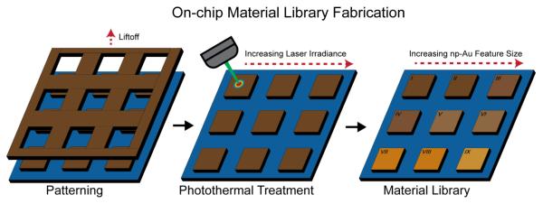
Figure 1.
Schematic illustrating the suggested process to be used for the fabrication of on-chip np-Au (brown) material libraries supported on silicon or glass (blue) using laser-based precise photothermal treatment to selectively anneal each np-Au pattern, resulting in an altered feature size (denoted by color change) on each pattern.

