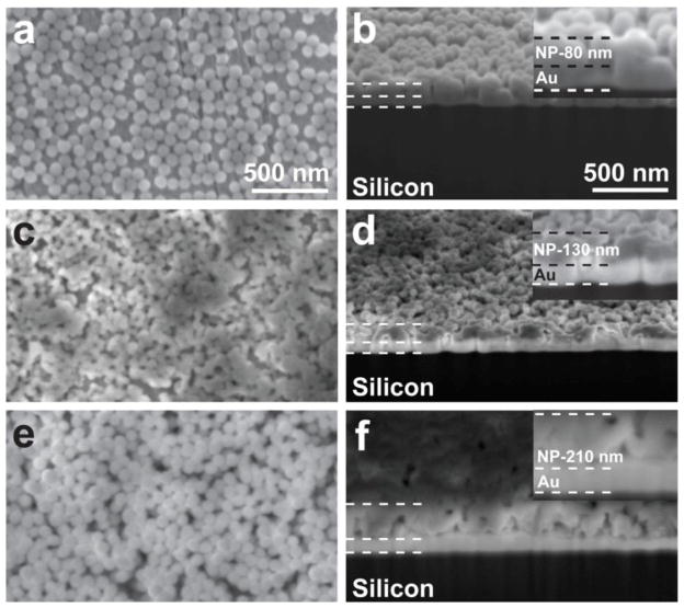
Figure 3.
SEM studies to determine the surface coverage and film thickness. The figure shows: (a) the 80 nm alkyne nanoparticle-deposited layer surface (plan view); (b) the cross sectional view of the 80 nm alkyne nanoparticle layer; (c) the 50 nm azide nanoparticle-layer surface (plan view) deposited on top of the first layer; (d) the cross sectional view of 50 nm azide nanoparticles layer deposited on top of the first layer; (e) the second 80 nm alkyne nanoparticle-deposited layer surface (third overall layer, plan view); and (f) the second cross sectional view of the three-layer system.

