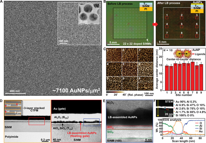
Fig. 2. Large-area and high-density assembly of AuNPs.
(A) TEM images of AuNPs assembled using the LB method. The insets show magnified TEM images. (B) Images before (left) and after (right) LB assembly of AuNPs on Tox. The insets show the corresponding schematics for the cross-sectional structure of the FG cell. (C) AFM images and quantitative spatial analysis of AuNPs assembled using the LB method at nine locations [right, red dashed boxes in (B)]. (D) TEM images of the CTFM (left). The inset shows a TEM image of the three-layer stacked CTFM. Magnified TEM image showing a detailed cross-sectional structure of the CTFM and uniform AuNP FG embedded in dielectrics (right, red box). (E) High-resolution TEM image showing a detailed structure of the dielectric-AuNP interface [blue box in (D)]. (F) Scanning TEM (STEM) image showing a cross-sectional structure of the CTFM (top left), quantitative EDS analysis results obtained at the spots marked in the STEM image with colored asterisks (top right), and EDS analysis results obtained along the yellow arrow shown in the STEM image (bottom).

