Figure 3.
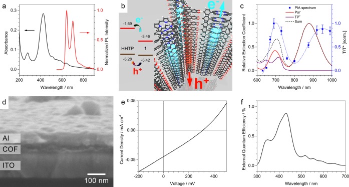
(a) Transmission absorption (black) and normalized PL (λexc = 405 nm, red) spectra of a TP-Por COF thin film. (b) Frontier orbital energies of the two COF subunits measured by DPV in solution and a schematic illustration of the photoinduced charge transfer. (c) PIA spectrum of the TP-Por COF film after excitation at 470 nm (blue squares; the blue line serves as a guide to the eye) together with the radical ion absorption spectra of Por– (red) and TP+ (purple) and their sum (black) assuming a 1:1 ratio of the two species. After photoexcitation, the TP-Por COF film shows two absorption bands in the range of the free radical ion absorption, indicating electron transfer from the donor to the acceptor moiety within the network (see the text). (d) Cross-sectional scanning electron micrograph of a TP-Por COF-based photovoltaic device showing the COF layer between the ITO and Al electrodes. The MoOx and ZnO contact layers are too thin to be visible in the micrograph. The current–voltage curve (e) and EQE spectrum (f) confirm the successful integration of the donor–acceptor COF as the active layer of the photovoltaic device.

