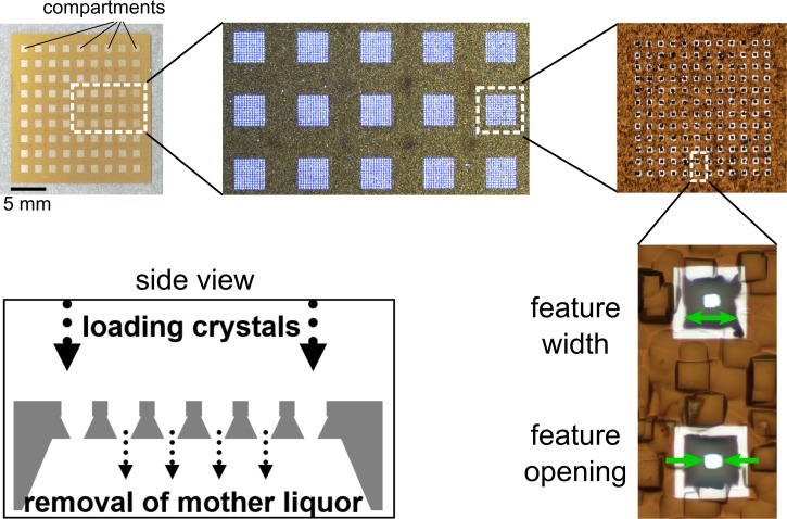
FIG. 1.
New crystallography chip design. The upper left picture shows a 20 × 20 mm chip with a 9 × 9 array of compartments. Each compartment is an array of tapered holes (“features,” 12 × 12 in the depicted chip). Two of the features are shown in the bottom right picture at high magnification. The width of the features at the top surface of the chip and the feature opening (width of the hole at the bottom surface) are indicated by green arrows. The structures in the surroundings are due to surface roughness of the unpolished Si substrate. They are also responsible for the grainy appearance of the substrate at lower magnifications. The white stripes around the features are a result of the fabrication process that leads to a local change in surface reflectivity. Side view: cross-section (schematic) along a line through the centers of the features in one row or column of a compartment (only 6 features are drawn, the real number of features per row/column is variable).

