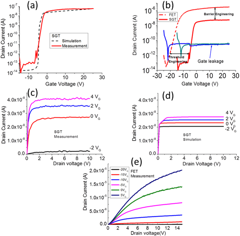
Figure 5.
(a) Experimental and simulated IDS-VGS curve of the SGT device at VDS = 1 V. (b) IDS-VGS curves from the Pt-ZnO (SGT) and Ti-ZnO (FET) curves of the same device at VDS = 1 V. Panel (b) also show the gate leakage current for both devices. (c) Experimental and (d) simulated output characteristics for the SGT device with VGS steps of 2 V between −2 to 4 V. (e) Output characteristics for the FET device with VGS steps of 5 V between −20 to 5 V.

