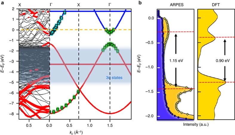
Figure 4. Band-structure of PPP polymers grown on Cu(110).
(a) DFT band structure (black lines, red circles correspond to the projection on the molecular layer), tight-binding modelling (red and blue solid lines), ARPES (green squares) and STS (blue squares) experimental dispersion curves. The absolute positions of the valence and conduction bands in the tight-binding model have been independently shifted towards the occupied states by 0.1 and 1.9 eV, respectively. (b) k-integrated photoemission DOS on the Cu(110) substrate (left panel, blue), on PPP/Cu(110) (left panel, yellow) and corresponding DFT DOS (right panel, yellow).

