
Figure 3. Colored SEM micrographs of different set of MAPbI3 nanowires.
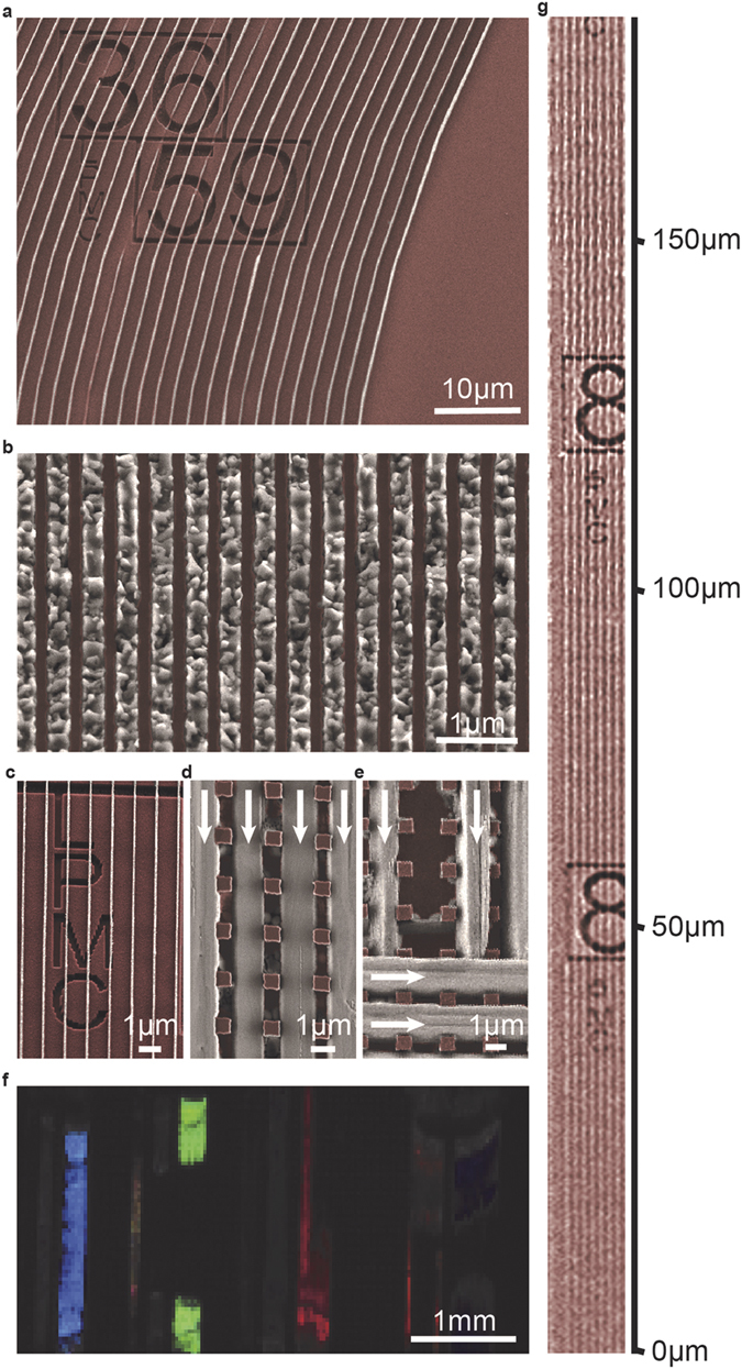
Curved nanowires after ZEP520A removal (a) dense array of aligned MAPbI3 nanoparticles (b) nanowires over etched patterns (c) perovskite nanowires grown with the guidance of Si pillars (d) that can be used to obtain cross-bar architectures; the growth directions are marked with arrows (e) Optical image of mm2-sized surfaces composed of MAPbI3 nanowires with different widths and spacings illuminated with white light. The blue, green, orange and red colors are due to the interference pattern of millimeter long periodic nanowire arrays (f and Video S2); extremely long, 200 nm-wide array of MAPbI3 nanowires on SiO2 after ZEP520A removal (g).