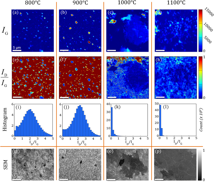
Figure 3. Characterization of the temperature dependent graphene growth morphologies.
(a–d) Raman integrated intensity maps of the graphitic, G, phonon mode (IG). Regions with significant IG values represent the presence of graphitic growth resolvable by the laser probe. A large graphene patch encompasses the Raman map obtained from the sample deposited at 1100 °C. All Raman maps are obtained from 25 μm × 25 μm areas. (e–h) Raman integrated intensity ratio maps of the D-peak relative to G-peak (ID/IG). The ID/IG maps reveal regions of high quality graphene growth (i.e. a reduction in relative number of defects). (i–l) Histograms of the ID/IG integrated Raman map raw data quantitate the transition to high quality graphene (ratios < 0.5) at deposition temperatures above 1000 °C. Counts for each ID/IG bin (0.2 in size) are three orders of magnitude (Count x103) higher than the scale bar suggests. (m–p) Representative SEM images of graphene films covering the nickel surface after deposition at each respective deposition temperature. The drastic increase in the size of graphene patches with constant layer thicknesses above 1000 °C is definitive, and for deposition of 1100 °C, distinct regions up to 100 μm in diameter were observed.

