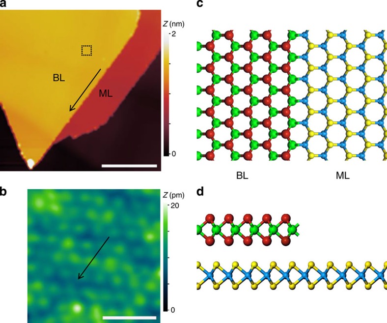
Figure 1. STM images and schematic models of BL–ML TMD lateral heterojunctions.
(a) STM image for a naturally formed BL–ML WSe2 HJ grown on HOPG by chemical vapour deposition. The bilayer and monolayer regions are labelled as shown. (b) Atomic resolution image taken on bilayer region where a dash square is labelled in a (not to scale). The sample biases and tunnelling currents used are (a) 3 V, 8 pA, (b) −1.0 V, 10 pA. The arrows in a and b indicate the zig-zag orientation of the bilayer–monolayer interface. (c,d) Schematic models of the BL–ML heterojunction viewing from top and side, respectively. The green and cyan represent the metal atoms in second and first layer respectively, while the red and yellow corresponding for chalcogen atoms. Scale bar, 100 nm (a); 1 nm (b).

